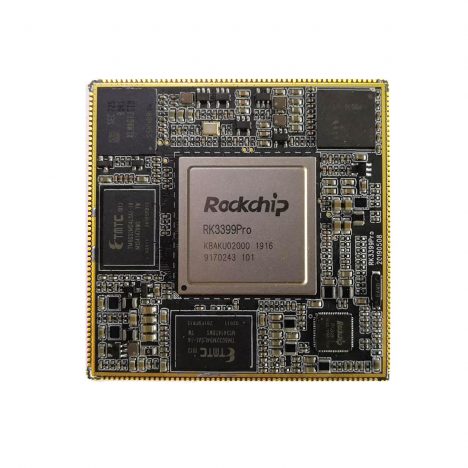
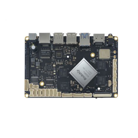
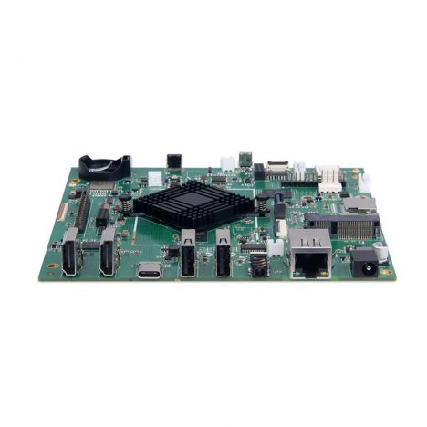
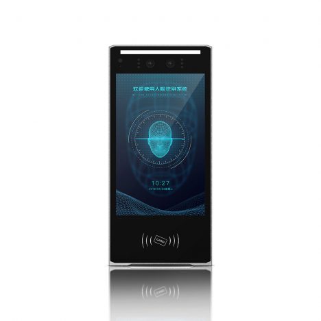
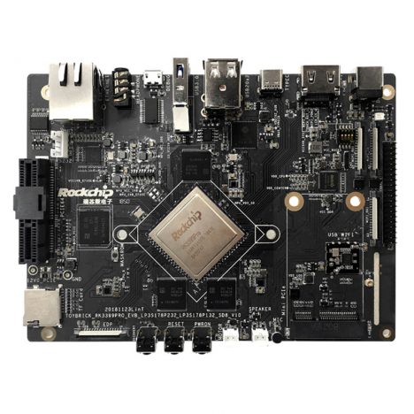
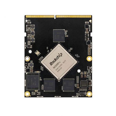
 瑞芯微RK3399Pro芯片简介
| RK3399Pro芯片主要参数 | |
| CPU | • 双Cortex-A72+四Cortex-A53 大小核CPU结构 |
| • 频率最高1.8GHz | |
| GPU | • Mali-T860MP4 GPU,支持OpenGL ES1.1/2.0/3.0/3.1, OpenVG1.1, OpenCL, DX11 |
| • 支持AFBC(帧缓冲压缩) | |
| NPU | • 支持8bit/16bit运算 |
| • 支持TensorFlow、Caffe模型 | |
| 内存 | • 双通道DDR3-1866/DDR3L-1866/LPDDR3-1866/LPDDR4 |
| • 支持eMMC 5.1,SDIO3.0 | |
| 多媒体 | • 支持4K VP9 and 4K 10bits H265/H264 视频解码,高达60fps |
| • 1080P 多格式视频解码 (VC-1, MPEG-1/2/4, VP8) | |
| • 1080P 视频编码,支持H.264,VP8格式 | |
| • 视频后期处理器:反交错、去噪、边缘/细节/色彩优化 | |
| 显示 | • 双VOP显示:分辨率分别支持4096×2160 及2560×1600 |
| • 支持双通道MIPI-DSI (每通道4线) | |
| • 显示支持:eDP 1.3(4 线,10.8Gbps) | |
| • HDMI 2.0支持4K 60Hz显示,支持HDCP 1.4/2.2 | |
| • 支持DisplayPort 1.2 (4 线,最高支持4K 60Hz) | |
| • 支持Rec.2020和Rec.709色域转换 | |
| 接口 | • 双ISP像素处理能力高达13MPix/s,支持双路摄像头数据同时输入 |
| • 支持USB3.0 Type-C接口 | |
| • 支持PCIe 2.1 (4 full-duplex lanes ) | |
| • 内置低功耗MCU | |
| • 支持8路数字麦克风阵列输入 | |
1.1 Overview
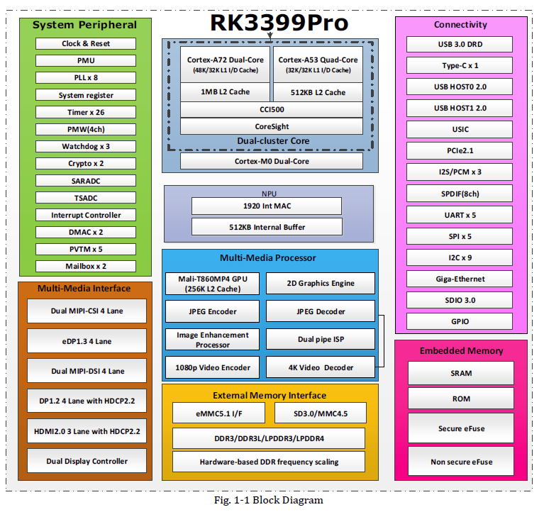
RK3399Pro is a low power, high performance processor for computing, personal mobile internet devices and other smart device applications. Based on Big.Little architecture, it integrates dual-core Cortex-A72 and quad-core Cortex-A53 with separate NEON coprocessor.
Equipped with one powerful neural network process unit(NPU), it supports mainstream platforms in the market, such as caffe, tensor flow, and so on.
Many embedded powerful hardware engines provide optimized performance for high-end application. RK3399Pro supports multi-format video decoders and encoders.
Embedded 3D GPU makes RK3399Pro completely compatible with OpenGL ES1.1/2.0/3.0/3.1, OpenCL and DirectX 11.1. Special 2D hardware engine with MMU will maximize display performance and provide very smooth operation.
1.2 Features The features listed below which may or may not be present in actual product, may be subject to the third party licensing requirements. Please contact Rockchip for actual product feature configurations and licensing requirements.
1.2.1 Microprocessor
Dual-core ARM Cortex-A72 MPCore processor and Quad-core ARM Cortex-A53 MPCore processor, both are high-performance, low-power and cached application processors
Two CPU clusters. Big cluster with dual-coreCortex-A72 is optimized for high-performance and little cluster with quad-core Cortex-A53 is optimized for low power.
Full implementation of the ARM architecture v8-A instruction set, ARM Neon Advanced SIMD (single instruction, multiple data) support for accelerating media and signal processing
ARMv8 Cryptography Extensions
CCI500 ensures the memory coherency between the two clusters
Each Cortex-A72 integrates 48KB L1 instruction cache and 32KB L1 data cache with 4-way set associative. Each Cortex A53 integrates 32KB L1 instruction cache and 32kB L1 data cache separately with 4-way set associative
1MB unified L2 Cache for Big cluster, 512KB unified L2 Cache for Little cluster
TrustZone technology support
Full CoreSight debug solution
Debug and trace visibility of whole systems
ETM trace support
Invasive and non-invasive debug
Eight separate power domains for CPU core system to support internal power switch and externally turn on/off based on different application scenario
PD_A72_B0: 1st Cortex-A72 + Neon + FPU + L1 I/D cache of big cluster
PD_A72_B1: 2nd Cortex-A72+ Neon + FPU + L1 I/D cache of big cluster
PD_SCU_B: SCU + L2 Cache controller, and including PD_A72_B0, PD_A72_B1, debug logic of big cluster
PD_A53_L0: 1st Cortex-A53 + Neon + FPU + L1 I/D Cache of little cluster
PD_A53_L1: 2nd Cortex-A53 + Neon + FPU + L1 I/D Cache of little cluster
PD_A53_L2: 3rd Cortex-A53 + Neon + FPU + L1 I/D Cache of little cluster
PD_A53_L3: 4th Cortex-A53 + Neon + FPU + L1 I/D Cache of little cluster
PD_SCU_L: SCU + L2 Cache controller, and including PD_A53_L0, PD_A53_L1, PD_A53_L2, PD_A53_L3, debug logic of little cluster
Two isolated voltage domain to support DVFS for big cluster and little cluster separately.
1.2.2 Neural Process Unit
Support 1920 Int8 MAC operations per cycle
Support 64 FP16 MAC operations per cycle
RK3399Pro Datasheet Rev 1.0
Support 192 Int16 MAC operations per cycle
512KB internal buffer
One isolated voltage domain to support DVFS
1.2.3 Boot
Support system boot from the following device :
SPI interface
eMMC interface
SD/MMC interface
Support system code download by the following interface:
USB OTG interface
1.2.4 Internal Memory
Internal BootROM
Size : 32KB
Internal SRAM
Size : 200KB
Support security and non-security access
Security or non-security space is software programmable
Security space can be 0KB,4KB,8KB,12KB,16KB,… up to 64KB by 4KB step
1.2.5 External Memory or Storage device
NPU Dedicated Dynamic Memory Interface (DDR3/DDR3L/LPDDR2/LPDDR3)
Compatible with JEDEC standards
Compatible with DDR3-1600/DDR3L-1600/ LPDDR2-1066 /LPDDR3-1600
Support 32-bit data width, 2 ranks (chip selects), max 2GB addressing space per rank, total addressing space is 2GB(max)
Dual-Channel Dynamic Memory Interface (DDR3/DDR3L/LPDDR3/LPDDR4) ①
Compatible with JEDEC standard DDR3-1866 /DDR3L-1866 /LPDDR3-1866 / LPDDR4 SDRAM
Support 2 channels, each channel is 16 or 32bits data width
Support up to 2 ranks (chip selects) for each channel; totally 4GB(max) address space. Maximum address space of one rank in a channel is also 4GB, which is software-configurable
eMMC Interface
Fully compliant with JEDEC eMMC 5.1and eMMC 5.0 specification
There is only one eMMC interface
It is backward compliant with eMMC 4.51 and earlier versions specification.
Supports HS400, HS200, DDR50 and legacy operating modes.
SD/MMC Interface
Compatible with SD3.0, MMC ver4.51
There are 2 MMC interfaces which can be configured as SD/MMC or SDIO
Data bus width is 4bits
1.2.6 System Component
Cortex-M0
Two Cortex-M0 inside RK3399Pro to cooperate with Cortex-A72/Cortex-A53
Fast code execution permits slower processor clock or increases sleep mode time
Deterministic, high-performance interrupt handling for time-critical applications
CRU (clock & reset unit)
Support clock gating control for individual components inside RK3399Pro
One oscillator with 24MHz clock input and 8 embedded PLLs
Support global soft-reset control for whole SOC, also individual soft-reset for every components
PMU (power management unit)
Multiple configurable work modes to save power by different frequency or automatic clock gating control or power domain on/off control
RK3399Pro Datasheet Rev 1.0
Lots of wakeup sources in different mode
6 separate voltage domains
30 separate power domains, which can be power up/down by software based on different application scenes
Timer
14 on-chip 64-bit Timers in SoC with interrupt-based operation for non-secure application
12 on-chip 64-bit Timers in SoC with interrupt-based operation for secure application
Provide two operation modes: free-running and user-defined count
Support timer work state checkable
Fixed 24MHz clock input
PWM
Four on-chip PWMs with interrupt-based operation
Embedded 32-bit timer/counter facility
Support capture mode
Support continuous mode or one-shot mode
Provides reference mode and output various duty-cycle waveform
Watchdog
Three Watchdogs in SoC with 32-bit counter width
Counter counts down from a preset value to 0 to indicate the occurrence of a timeout
WDT can perform two types of operations when timeout occurs:
Generate a system reset
First generate an interrupt and if this is not cleared by the service routine by the time a second timeout occurs then generate a system reset
Programmable reset pulse length
Totally 16 defined-ranges of main timeout period
Mailbox
Two Mailboxes in SoC to service multi-core communication
Support four mailbox elements per mailbox, each element includes one data word, one command word register and one flag bit that can represent one interrupt
Provide 32 lock registers for software to use to indicate whether mailbox is occupied
Bus Architecture
128-bit/64-bit/32-bit multi-layer AXI/AHB/APB composite bus architecture
CCI500 embedded to support two clusters cache coherency
Interrupt Controller
Support 8 PPI interrupt source and 148 SPI interrupt sources input from different components inside RK3399Pro
Support 16 software-triggered interrupts
Input interrupt level is fixed, high-level sensitive for SPI and low-level sensitive for PPI
Support Locality-specific Peripheral Interrupts (LPIs). These interrupts are generated by a peripheral writing to a memory-mapped register in the controller
Two AXI stream interrupt interfaces separately for each cluster
Support different interrupt priority for each interrupt source, and they are always software-programmable
DMAC
Linked list DMA function is supported to complete scatter-gather transfer
Support data transfer types with memory-to-memory, memory-to-peripheral, peripheral-to-memory
Signals the occurrence of various DMA events using the interrupt output signals
Mapping relationship between each channel and different interrupt outputs is software-programmable
Two embedded DMA controller, BUS_DMAC is for bus system, PERI_DMAC is for peripheral system
DMAC0 features:
6 channels totally
10 hardware request from peripherals
2 interrupt output
RK3399Pro Datasheet Rev 1.0
Support TrustZone technology and programmable secure state for each DMA channel
DMAC1 features:
8 channels totally
20 hardware request from peripherals
2 interrupt output
Support TrustZone technology and programmable secure state for each DMA channel
Security system
Support TrustZone technology for the following components inside RK3399Pro
Cortex-A72, support security and non-security mode, switch by software
Cortex-A53, support security and non-security mode, switch by software
Except Cortex-A72 and Cortex-A53, the other masters in the SoC can also support security and non-security mode by software-programmable
Some slave components in SoC can only be addressed by security master and the other slave components can be addressed by security master or non-security master by software-programmable
Internal memory, part of space is addressed only in security mode, detailed size is software-programmable together with TZMA (TrustZone memory adapter)
External DDR space can be divided into eight parts; each part can be software-programmable to be addressed in security mode or non-security mode
Embedded dual-channel encryption and decryption engine
Support AES 128/192/256-bit key mode, ECB/CBC/CTR/XTS chain mode, Slave/FIFO mode
Support DES/3DES (ECB and CBC chain mode), 3DES (EDE/EEE key mode), Slave/FIFO mode
Support SHA1/SHA256/MD5(with hardware padding) HASH function, FIFO mode only
Support 160-bit Pseudo Random Number Generator (PRNG)
Support 256-bit True Random Number Generator (TRNG)
Support PKA 512/1024/2048-bit Exp Modulator
Support security boot
Support security debug
1.2.7 Video CODEC
Video Decoder
H.264/AVC, Base/Main/High/High10 profile @ level 5.1; up to 4Kx2K @ 30fps
H.265/HEVC, Main/Main10 profile @ level 5.1 High-tier; up to 4Kx2K @ 60fps
VP9, profile 0, up to 4Kx2K @ 60fps
MPEG-1, ISO/IEC 11172-2, up to 1080P @ 60fps
MPEG-2, ISO/IEC 13818-2, SP@ML, MP@HL, up to 1080P @ 60fps
MPEG-4, ISO/IEC 14496-2, SP@L0-3, ASP@L0-5, up to 1080P @ 60fps
VC-1, SP@ML, MP@HL, AP@L0-3, up to 1080P @ 60fps
MVC is supported based on H.264 or H.265, up to 1080P @ 60fps
Output data format YUV420 semi-planar, YUV400(monochrome), YUV422 is supported by H.264
For MPEG-4, GMC (global motion compensation) not supported
For VC-1, up-scaling and range mapping are supported in image post-processor
Video Encoder
Support video encoder for H.264 UP to HP@level4.1, MVC and VP8
Only support I and P slices, not B slices
Input data format:
YCbCr 4:2:0 planar
YCbCr 4:2:0 semi-planar
YCbYCr 4:2:2
CbYCrY 4:2:2 interleaved
RGB444 and BGR444
RK3399Pro Datasheet Rev 1.0
RGB555 and BGR555
RGB565 and BGR565
RGB888 and BRG888
RGB101010 and BRG101010
Image size is from 96×96 to 1920×1080(Full HD)
Maximum frame rate is up to 1920×1080@30FPS②
1.2.8 JPEG CODEC
JPEG Decoder
Input JPEG file: YCbCr 4:0:0, 4:2:0, 4:2:2, 4:4:0, 4:1:1 and 4:4:4 sampling formats
Output raw image: YCbCr 4:0:0, 4:2:0, 4:2:2, 4:4:0, 4:1:1 and 4:4:4 semi-planar
Decoder size is from 48×48 to 8176×8176(66.8Mpixels)
Support JPEG ROI (region of image) decode
Maximum data rate③ is up to 76million pixels per second
Embedded memory management unit(MMU)
JPEG Encoder
Input raw image:
YCbCr 4:2:0 planar
YCbCr 4:2:0 semi-planar
YCbYCr 4:2:2
CbYCrY 4:2:2 interleaved
RGB444 and BGR444
RGB555 and BGR555
RGB565 and BGR565
RGB888 and BRG888
RGB101010 and BRG101010
Output JPEG file: JFIF file format 1.02 or Non-progressive JPEG
Encoder image size up to 8192×8192(64million pixels) from 96×32
Maximum data rate③ up to 90million pixels per second
1.2.9 Image Enhancement-Processor (IEP)
Image format
Input data: XRGB/RGB565/YUV420/YUV422
Output data: ARGB/RGB565/YUV420/YUV422
Max resolution for dynamic image
De-interlace: 1920×1080
Sampling noise reduction: 1920×1080
Compression noise reduction: 4096×2304
Enhancement: 4096×2304
Enhancement
Gamma adjustment with programmable mapping table
Hue/Saturation/Brightness/Contrast enhancement
Programmable distance table for detail and edge enhancement
Noise reduction
Spatial sampling noise reduction
Temporal sampling noise reduction
De-interlace
Input 4 fields, output 2 frames mode
Input 4 fields, output 1 frames mode
Input 2 fields, output 1 frames mode
1.2.10 Graphics Engine
3D Graphics Engine:
ARM Mali-T860MP4 GPU, support OpenGL ES1.1/2.0/3.0, OpenCL1.2, DirectX11.1 etc.
Embedded 4 shader cores with shared hierarchical tiler
RK3399Pro Datasheet Rev 1.0
Provide MMU and L2 Cache with 256KB size
2D Graphics Engine:
Data format
Support input of ARGB/RGB888/RGB565/RGB4444/RGB5551/YUV420/YUV422
Support input of YUV422SP(10-bit)/YUV420SP(10-bit)
Support output of ARGB/RGB888/RGB565/RGB4444/RGB5551/YUV420/YUV422
Support output of YVYU422/420
Max resolution: 8192×8192 source, 4096×4096 destination
Scaling
Support scaling up and down
Arbitrary non-integer scaling ratio,from 1/16 to 16
Rotation
0, 90, 180, 270 degree rotation
x-mirror, y-mirror& rotation operation
BitBLT
Alpha Blending
1.2.11 Video IN/OUT
Camera Interface
One or two MIPI-CSI input interface
Image Signal Processer
Input interface
DVP interface
ITU-R BT601/656 with raw8/raw10/raw12
MIPI interface
Support x1/x2/x4 DPHY RX data lanes
Support RAW8, RAW10, RAW12
Maximum input resolution is 4416×3312
ISP process
Support Black level compensation
Support 4 channels of Lens shade correction
Support AF/AWB/AE/Hist
Output interface
Support output format :
YUV422sp/YUV420sp, with UV swap
RGB888/RGB666/RGB565
RAW8/RAW12
Display Interface
Embedded two VOP, output from the following display interface.
Two MIPI-DSI port, and one of which can be configured with MIPI-CSI2
One eDP port
One DP port
One HDMI port
Support AFBC function co-operation with GPU
Video Output Processor(VOP_BIG)
Display interface
HDMI interface
Support 480p/480i/576p/576i/720p/1080p/1080i/4k
Support RGB/YUV420(up to 10-bit) format
DP interface
Support progressive/interlace
Support RGB/YUV420/YUV422/YUV444(up to 10-bit) format
MIPI interface
MIPI DCS command mode
Dual-MIPI
EDP interface
Max resolution
RK3399Pro Datasheet Rev 1.0
Max input resolution:4096×2304
Max output resolution:4096×2160
Scanning timing 8192×4096
Support configurable polarity of DCLK/HSYNC/VSYNC/DEN
Display process
GAMMA
X-MIRROR, Y-MIRROR
Post scale down for TV over scan
Layer process
Background layer
programmable 30-bit color
Afbcd
format: ARGB8888/RGB888/RGB565
win_sel(win0/win1/win2/win3)
Win0/Win1 layer
Support data format
RGB888, ARGB888, RGB565,
YCbCr420SP, YCbCr422SP, CbCr444SP, YUYV420, YUYV422,YVYU420, YVYU422
RGB(8-bit), YUV(8-bit/10-bit), YVYU/YUYV(8-bit)
Support 1/8 to 8 scaling-down and scaling-up engine
Win2/Win3 layer
Support data format
RGB888, ARGB888, RGB565
8BPP
4 display regions
only one region at one scanning line
Hardware Cursor layer
Support data format
RGB888, ARGB888, RGB565
8BPP
Overlay
support RGB and YUV domain overlay
Support 6 layers, background/win0/win1/win2/win3/hwc
Alpha blending
Write back
Support format
RGB565(8-bit), RGB888P(8-bit)
YUV420(8-bit)
Support scale
horizontal scale down, 0.25~1.0
vertical throw odd/even line
Video Output Processor(VOP_LIT)
Display interface
HDMI interface
Support 480p/480i/576p/576i/720p/1080p/1080i
Support RGB format
DP interface
Support progressive/interlace
Support RGB/YUV420/YUV422/YUV444format
MIPI interface
MIPI DCS command mode
Dual-MIPI
EDP interface
Max resolution
Max input resolution:4096×2304
Max output resolution:2560×1600
RK3399Pro Datasheet Rev 1.0
Scanning timing 8192×4096
Support configurable polarity of DCLK/HSYNC/VSYNC/DEN
Display process
GAMMA
X-MIRROR, Y-MIRROR
Post scale down for TV overscan
Layer process
Background layer
Programmable 30-bit color
Win0 layer
Support data format
RGB888, ARGB888, RGB565,
YCbCr420SP, YCbCr422SP, CbCr444SP, YUYV420, YUYV422,YVYU420, YVYU422
RGB(8-bit), YUV(8-bit), YVYU/YUYV(8-bit)
Support 1/8 to 8 scaling-down and scaling-up engine
Win2 layer
Support data format
RGB888, ARGB888, RGB565
8BPP
4 display regions
only one region at one scanning line
Hardware Cursor layer
Support data format
RGB888, ARGB888, RGB565
8BPP
Support four hwc size: 32×32,64×64,96×96,128×128
Overlay
support RGB and YUV domain overlay
Support 4 layers, background/win0/win2/hwc
Alpha blending
1.2.12 HDMI
Single Physical Layer PHY with support for HDMI 1.4 and 2.0 operation
Support HDCP 1.4/2.2
1.2.13 MIPI PHY
Embedded 3 MIPI PHY, MIPI0 only for DSI, MIPI1 for DSI or CSI, MIPI2 only for CSI
Lane operation ranging from 80 Mbps to 1.5 Gbps in forward direction
Each port has 4 data lane, providing up to 6.0 Gbps data rate
1.2.14 eDP PHY
Compliant with eDPTM Specification, version 1.3
Up to 4 physical lanes of 2.7/1.62 Gbps/lane
Hot plug and unplug detection and link status monitor
Support Panel Self Refresh(PSR)
1.2.15 DisplayPort
Compliant with DisplayPort Specification, version 1.2
Compliant with HDCP2.2 (and compatible with HDCP1.3)
There is only one DisplayPort controller built-in RK3399Pro which is shared by Type-C interface
Supports up to 4kx2k @60fps resolution
Variety of audio formats–PCM and compressed, over I2S or SPDIF interfaces
1Mbps AUX channel
RK3399Pro Datasheet Rev 1.0
1.2.16 TYPE-C Interface
Embedded 1 Type-C PHY
Compliant with USB Type-C Specification, revision 1.1
Compliant with USB Power Delivery Specification, revision 2.0
Attach/detach detection and signaling as DFP, UFP and DRP
Plug orientation/cable twist detection
Enable/disable VBUS as DFP and DRP (when operating as DFP)
VBUS detection as UFP and DRP (when operating as UFP)
USB Power Delivery communication across the CC wire
Support USB3.0 Type-C and DisplayPort 1.2 Alt Mode on USB Type-C. Two PMA TX-only lanes and two PMA half-duplex TX/RX lanes (can be configured as TX-only or RX-only)
Up to 5Gbps data rate for USB3.0
Up to 5.4Gbps(HBR2) data rate for DP1.2, can support 1/2/4lane mode
Support DisplayPort AUX channel
1.2.17 Audio Interface
I2S/PCM
Three I2S/PCM in SoC
I2S0/I2S2 support up to 8 channels TX and 8 channels RX. I2S1 supports up to 2 channels TX and 2 channels RX
I2S2 is connected to HDMI and DisplayPort internally. I2S0 and I2S1 are exposed for peripherals.
Audio resolution from 16bits to 32bits
Sample rate up to 192KHz
Provides master and slave work mode, software configurable
Support 3 I2S formats (normal, left-justified, right-justified)
Support 4 PCM formats (early, late1, late2, late3)
I2S and PCM mode cannot be used at the same time
SPDIF
Support two 16-bit audio data store together in one 32-bit wide location
Support biphase format stereo audio data output
Support 16 to 31-bit audio data left or right justified in 32-bit wide sample data buffer
Support 16, 20, 24-bit audio data transfer in linear PCM mode
Support non-linear PCM transfer
1.2.18 Connectivity
SDIO interface
Compatible with SDIO 3.0 protocol
4bits data bus width
There are 2 total MMC interfaces which may be configured as SD/MMC or SDIO
GMAC 10/100/1000M ethernet controller
Supports 10/100/1000-Mbps RGMII interfaces and 10/100-Mbps RMII interface
Supports both full-duplex and half-duplex operation
Supports CSMA/CD Protocol for half-duplex operation
Supports packet bursting and frame extension in 1000 Mbps half-duplex operation
Supports IEEE 802.3x flow control for full-duplex operation
Preamble and start-of-frame data (SFD) insertion in Transmit, and deletion in receive paths
Automatic CRC and pad generation controllable on a per-frame basis
Options for Automatic Pad/CRC Stripping on receive frames
Programmable fame length to support Standard Ethernet frames
Supports IEEE 802.1Q VLAN tag detection for reception frames
Support detection of LAN wake-up frames and AMD Magic Packet frames
MDIO Master interface for PHY device configuration and management
Support detection of LAN wake-up frames and AMD Magic Packet frames
RK3399Pro Datasheet Rev 1.0
SPI Controller
5 on-chip SPI controllers are inside
Support serial-master and serial-slave mode, software-configurable
DMA-based or interrupt-based operation
UART Controller
5 on-chip UART controllers inside RK3399Pro
DMA-based or interrupt-based operation
Support 5bits,6bits,7bits,8bits serial data transmit or receive
Standard asynchronous communication bits such as start,stop and parity
Support different input clock for UART operation to get up to 4Mbps or other special baud rate
Support non-integer clock divides for baud clock generation
Support auto flow control mode for UART0 and UART3
I2C controller
9 on-chip I2C controllers
Multi-master I2C operation
Support 7bits and 10bits address mode
Serial 8bits oriented and bidirectional data transfers can be made
Software programmable clock frequency
Data on the I2C-bus can be transferred at rates of up to 100KHz in the Standard-mode, up to 400KHz in the Fast-mode or up to 1MHz in Fast-mode Plus.
GPIO
5 groups of GPIO (GPIO0~GPIO4)
All of GPIOs can be used to generate interrupt to CPU
GPIO0 and GPIO1 can be used to wakeup system from low-power mode
The pull direction (pull-up or pull-down) for all of GPIOs are software-programmable
All of GPIOs are always in input direction in default after power-on-reset
The drive strength for all of GPIOs is software-programmable
USB 3.0 DRD
Embedded 1 USB 3.0 interfaces
Compatible with USB3.0 Specification
Universal Serial Bus 3.0 Specification, Revision 1.0
Universal Serial Bus Specification, Revision 2.0
Extensible Host Controller Interface for Universal Serial Bus (xHCI), Revision 1.1
Support Control/Bulk (including stream)/Interrupt/Isochronous Transfer
Supports super-speed (5Gbps)
Descriptor Caching and Data Pre-fetching
USB 3.0 xHCI Host Features
Support up to 64 devices
Support 1 interrupter
Support 1 USB2.0 port and 1 Super-Speed port
Concurrent USB3.0/USB2.0 traffic, up to 8.48Gbps bandwidth
Support standard or open-source xHCI and class driver
Support xHCI Debug Capability
USB 3.0 Dual-Role Device (DRD) Features
Static Device operation
Static Host operation
USB3.0/USB2.0 OTG A device and B device basing on ID
UFP/DFP and Data Role Swap Defined in USB TypeC Specification
Not support USB3.0/USB2.0 OTG session request protocol(SRP), host negotiation protocol(HNP) and Role Swap Protocol(RSP)
USB 2.0 Host
Embedded 2 USB 2.0 Host interfaces
Compatible with USB 2.0Host specification
Supports high-speed(480Mbps), full-speed(12Mbps) and low-speed(1.5Mbps) mode
Provides 16 host mode channels
Support periodic out channel in host mode
RK3399Pro Datasheet Rev 1.0
PCIe
One PCIe port in RK3399Pro
Compatible with PCI Express Base Specification Revision 2.1
Dual operation mode: Root Complex(RC)and End Point(EP)
Maximum link width is 4, single bi-directional Link interface
Support 2.5Gbps serial data transmission rate per lane per direction
Support Single Physical PCI Functions in Endpoint Mode
Support Legacy Interrupt and MSI and MSI-X interrupt
1.2.19 Others
Temperature Sensor(TSADC)
Embedded 2 channel TSADC in RK3399Pro
TSADC clock must be less than 800KHz
10-bit TSADC up to 50Ksps sampling rate
-40~125C temperature range and 5℃ temperature resolution
Successive Approximation Register(SARADC)
6-channel single-ended 10-bit SAR analog-to-digital converter
SARADC clock must be less than 13MHz
Conversion speed range is up to 1Msps sampling rate
eFuse
Two 1024bits(32×32) high-density electrical Fuse are integrated in RK3399Pro
Support standby mode and power down mode
Embedded power-switch
Embedded four redundancy bits
Package Type
FCBGA1372(body: 27mmx27mm; ball size: 0.35mm)
Notes :① : DDR3/DDR3L/LPDDR3/LPDDR4 could not be used simultaneously
②:Actual maximum frame rate will depend on the clock frequency and system bus performance
③:Actual maximum data rate will depend on the clock frequency and JPEG compression rate
RK3399Pro Datasheet Rev 1.0
