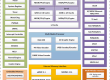
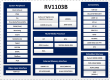
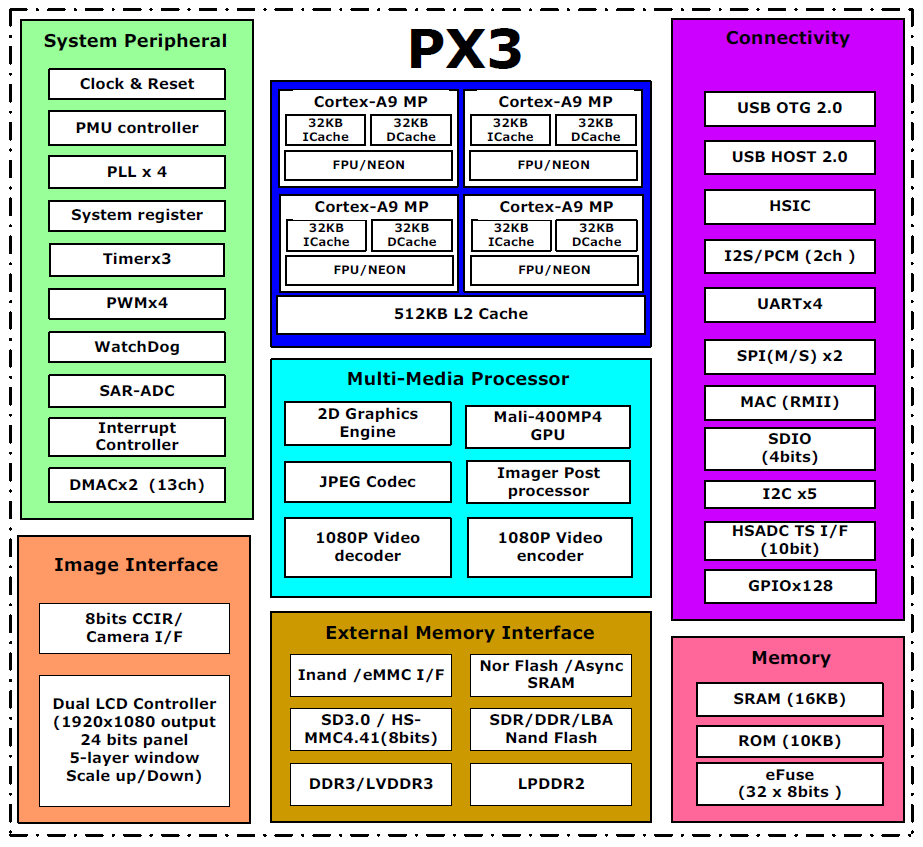
PX3是一款低功耗、高性能的车载信息娱乐系统处理器,支持基于ARM Cortex架构的Android,包括四核Cortex-A9,分别配备NEON和FPU协处理器。许多功能强大的嵌入式硬件引擎为高端应用提供了优化的性能。PX3支持几乎全格式的视频解码器1080p@60fps,还支持H.264/MVC/VP8编码器1080p@30fps,高品质JPEG编码器/解码器,以及专用的图像预处理器和后处理器。
Embedded 3D GPU makes PX3 completely compatible with OpenGL ES2.0 and 1.1,OpenVG1.1. Special 2D hardware engine with MMU will maximize display performance and provide very smoothly operation.PX3 has high-performance external memory interface (DDR3/LPDDR2/LVDDR3) capable of sustaining demanding memory bandwidths, also provides a complete set of peripheral interface to support very flexible applications.
1.2 Features
The features listed below which may or may not be present in actual product, may be subject to
the third party licensing requirements. Please contact Rockchip for actual product feature
configurations and licensing requirements.
1.2.1 Processor
Quad-core ARM Cortex-A9 MP Core processor, a high-performance, low-power and cached
application processor
Full implementation of the ARM architecture v7-A instruction set, ARM Neon Advanced
SIMD (single instruction, multiple data) support for accelerated media and signal
processing computation
Superscalar, variable length, out-of-order pipeline with dynamic branch prediction, 8-stage
pipeline
Include VFPv3 hardware to support single and double-precision add, subtract, divide,
multiply and accumulate, and square root operations
SCU ensures memory coherency between the four CPUs
Integrated timer and watchdog timer per CPU
Integrated 32KB L1 instruction cache , 32KB L1 data cache with 4-way set associative
512KB unified L2 Cache
Trustzone technology support
Full core sight debug solution
Debug and trace visibility of whole systems
ETM trace support
Invasive and non-invasive debug
Six separate power domains for every core to support internal power switch and externally
turn on/off based on different application scenario
PD_A9_0: 1st Cortex-A9 + Neon + FPU + L1 I/D Cache
PD_A9_1: 2nd Cortex-A9 + Neon + FPU + L1 I/D Cache
PD_A9_2: 3rd Cortex-A9 + Neon + FPU + L1 I/D Cache
PD_A9_3: 4th Cortex-A9 + Neon + FPU + L1 I/D Cache
PD_DBG: Core Sight-DK for Cortex-A9
PD_SCU: SCU + L2 Cache controller + L2 Dataram, and including PD_A9_0, PD_A9_1,
PD_A9_2, PD_A9_3, PD_DGB
One isolated voltage domain to support DVFS
1.2.2 Memory Organization
Internal on-chip memory
10KB Boot Rom
PX3 Datasheet Rev 1.4
Copyright 2016 @Fuzhou Rockchip Electronics Co., Ltd. 8
32KB internal SRAM for security and non-security access, detailed size is
programmable
External off-chip memory①
DDR3-1066, 16/32bits data widths, 2 ranks, totally 2GB(max) address space,
maximum address space for one rank is also 2GB.
LPDDR2-1066, 32bits data width, 2 ranks, totally 2GB(max) address space, maximum
address space for one rank is also 2GB.
Async SRAM/Nor Flash, 8/16bits data width,2banks
Async Nand Flash(include LBA Nand), 8/16bits data width, 4 banks, 60bits ECC
Sync ONFI Nand Flash , 8bits data width, 8 banks, 60bits ECC
1.2.2 Internal Memory
Internal BootRom
Size : 10KB
Support system boot from the following device:
8bits/16bits Async Nand Flash
8bits ONFI Nand Flash
SPI0 interface
eMMC interface
SDMMC interface
Support system code download by the following interface:
USB OTG interface
UART2Interface
Internal SRAM
Size : 32KB
Support security and non-security access
Security or non-security space is software programmable
Security space can be 0KB,4KB,8KB,12KB,16KB,32KB continuous size
1.2.3 External Memory or Storage device
Dynamic Memory Interface (DDR3/LPDDR2)
Compatible with JEDEC standard DDR3/LPDDR2 SDRAM
Data rates up to 1066Mbps(533MHz) for DDR3/LPDDR2
Support up to 2 ranks (chip selects), totally 2GB(max) address space, and maximum
address space for one rank is also 2GB, which is software-configurable.
16bits/32bits data width is software programmable
7 host ports with 64bits AXI bus interface for system access, AXI bus clock is
asynchronous with DDR clock
Programmable timing parameters to support DDR3/LPDDR2 SDRAM from various
vendor
Advanced command reordering and scheduling to maximize bus utilization
Low power modes, such as power-down and self-refresh for DDR3/LPDDR2 SDRAM;
clock stop and deep power-down forLPDDR2 SDRAM
Compensation for board delays and variable latencies through programmable pipelines
Embedded dynamic drift detection in the PHY to get dynamic drift compensation with
the controller
Programmable output and ODT impedance with dynamic PVT compensation
Support one low-power work mode: power down DDR PHY and most of DDR IO except
two CS and two CKE output signals, make SDRAM still in self-refresh state to prevent
data missing.
Static Memory Interface (ASRAM/Nor Flash)
Compatible with standard async SRAM or Nor Flash
Support up to 2 banks (chip selects)
For bank0, 8bits/16bits data width is software programmable; For bank1, 16bits data
width is fixed
Support separately data and address bus, also support shared data and address bus to
PX3 Datasheet Rev 1.4
Copyright 2016 @Fuzhou Rockchip Electronics Co., Ltd. 9
save IO numbers
Nand Flash Interface
Support 8bits/16bits async nand flash, up to 4 banks
Support 8bits sync DDR nand flash, up to 4 banks
Support LBA nand flash in async or sync mode
Up to 60bits hardware ECC
For DDR nand flash, support DLL bypass and 1/4 or 1/8 clock adjust, maximum clock
rate is 75MHz
For async nand flash, support configurable interface timing , maximum data rate is
16bit/cycle
Embedded special DMA interface to do data transfer
Also support data transfer together with general DMAC1 in SoC system
eMMC Interface
Compatible with standard iNAND interface
Support MMC4.41 protocol
Provide eMMC boot sequence to receive boot data from external eMMC device
Support combined single FIFO(32x32bits) for both transmit and receive operations
Support FIFO over-run and under-run prevention by stopping card clock automatically
Support CRC generation and error detection
Embedded clock frequency division control to provide programmable baud rate
Support block size from 1 to 65535Bytes
8bits data bus width
SD/MMC Interface
Compatible with SD3.0, MMC ver4.41
Support combined single FIFO(32x32bits) for both transmit and receive operations
Support FIFO over-run and under-run prevention by stopping card clock automatically
Support CRC generation and error detection
Embedded clock frequency division control to provide programmable baud rate
Support block size from 1 to 65535Bytes
Data bus width is 4bits
1.2.4 System Component
CRU (clock & reset unit)
Support clock gating control for individual components inside PX3
One oscillator with 24MHz clock input and 4 embedded PLLs
Up to 2.2GHz clock output for all PLLs
Support global soft-reset control for whole SOC, also individual soft-reset for every
components
PMU(power management unit)
6 work modes(slow mode, normal mode, idle mode, stop mode, sleep mode, power-off
mode) to save power by different frequency or automatic clock gating control or power
domain on/off control
Lots of wakeup sources in different mode
3 separate voltage domains
10 separate power domains, which can be power up/down by software based on
different application scenes
Timer
7 on-chip 64bits Timers in SoC with interrupt-based operation
Provide two operation modes: free-running and user-defined count
Support timer work state checkable
Fixed 24MHz clock input
PX3 Datasheet Rev 1.4
Copyright 2016 @Fuzhou Rockchip Electronics Co., Ltd. 10
PWM
Four on-chip PWMs with interrupt-based operation
Programmable 4-bit pre-scalar from APB bus clock
Embedded 32-bit timer/counter facility
Support single-run or continuous-run PWM mode
Provides reference mode and output various duty-cycle waveform
WatchDog
32 bits watchdog counter width
Counter clock is from APB bus clock
Counter counts down from a preset value to 0 to indicate the occurrence of a timeout
WDT can perform two types of operations when timeout occurs:
Generate a system reset
First generate an interrupt and if this is not cleared by the service routine by the
time a second timeout occurs then generate a system reset
Programmable reset pulse length
Totally 16 defined-ranges of main timeout period
Bus Architecture
64-bit multi-layer AXI/AHB/APB composite bus architecture
5 embedded AXI interconnect
CPU interconnect with three 64-bits AXI masters, two 64-bits AXI slaves, one
32-bits AHB master and lots of 32-bits AHB/APB slaves
PERI interconnect with two 64-bits AXI masters, one 64-bits AXI slave, one 32-bits
AXI slave, four 32-bits AHB masters and lots of 32-bits AHB/APB slaves
Display interconnect with six 64-bits AXI masters and one 32-bits AHB slave
GPU interconnect with one 128-bits AXI master and 64-bits AXI slave ,they are
point-to-point AXI-lite architecture
VCODEC interconnect also with one 64-bits AXI master and one 32-bits AHB
slave ,they are point-to-point AXI-lite architecture
For each interconnect with AXI/AHB/APB composite bus, clocks for AXI/AHB/APB
domains are always synchronous, and different integer ratio is supported for them.
Flexible different QoS solution to improve the utility of bus bandwidth
Interrupt Controller
Support 3 PPI interrupt source and 76 SPI interrupt sources input from different
components inside PX3
Support 16 software-triggered interrupts
Input interrupt level is fixed , only high-level sensitive
Two interrupt outputs (nFIQ and nIRQ) separately for each Cortex-A9, both are
low-level sensitive
Support different interrupt priority for each interrupt source, and they are always
software-programmable
DMAC
Micro-code programming based DMA
The specific instruction set provides flexibility for programming DMA transfers
Linked list DMA function is supported to complete scatter-gather transfer
Support internal instruction cache
Embedded DMA manager thread
Support data transfer types with memory-to-memory, memory-to-peripheral,
peripheral-to-memory
Signals the occurrence of various DMA events using the interrupt output signals
Mapping relationship between each channel and different interrupt outputs is
software-programmable
Two embedded DMA controller , DMAC0 is for CPU system, DMAC1 is for peri system
DMAC0 features:
6 channels totally
PX3 Datasheet Rev 1.4
Copyright 2016 @Fuzhou Rockchip Electronics Co., Ltd. 11
11 hardware request from peripherals
2 interrupt output
Dual APB slave interface for register configure, designated as secure and
non-secure
Support Trustzone technology and programmable secure state for each DMA
channel
DMAC1 features:
7 channels totally
13 hardware request from peripherals
2 interrupt outputs
Not support trustzone technology
Security system
Support trustzone technology for the following components inside PX3
Cortex-A9, support security and non-security mode, switch by software
DMAC0, support some dedicated channels work only in security mode
eFuse, only accessed by Cortex-A9 in security mode
Internal memory , part of space is addressed only in security mode, detailed size is
software-programmable together with TZMA(trustzone memory adapter) and
TZPC(trustzone protection controller)
1.2.5 Video CODEC
Shared internal memory and bus interface for video decoder and encoder②
Real-time video decoder of MPEG-1, MPEG-2, MPEG-4,H.263, H.264 , AVS , VC-1 , VP8 ,
MVC
Error detection and concealment support for all video formats
Output data format is YUV420 semi-planar, and YUV400(monochrome) is also
supported for H.264
H.264 up to HP level 4.2 : 1080p@60fps (1920×1088)③
MPEG-4 up to ASP level 5 : 1080p@60fps (1920×1088)
MPEG-2 up to MP : 1080p@60fps (1920×1088)
MPEG-1 up to MP : 1080p@60fps (1920×1088)
H.263 : 576p@60fps(720×576)
VC-1 up to AP level 3 : 1080p@30fps (1920×1088)
VP8 : 1080p@60fps (1920×1088)
AVS : 1080p@60fps (1920×1088)
MVC : 1080p@60fps (1920×1088)
For AVS, 4:4:4 sampling not supported
For H.264, Image cropping not supported
For MPEG-4,GMC(global motion compensation) not supported
For VC-1, up scaling and range mapping are supported in image post-processor
For MPEG-4 SP/H.263, using a modified H.264 in-loop filter to implement deblocking
filter in post-processor unit
1.2.6 Video Encoder
Support video encoder for H.264 (BP@level4.0, MP@level4.0, HP@level4.0), MVC and
VP8
Only support I and P slices, not B slices
Support error resilience based on constrained intra prediction and slices
Input data format :
YCbCr 4:2:0 planar
YCbCr 4:2:0 semi-planar
YCbYCr 4:2:2
CbYCrY 4:2:2 interleaved
RGB444 and BGR444
RGB555 and BGR555
RGB565 and BGR565
PX3 Datasheet Rev 1.4
Copyright 2016 @Fuzhou Rockchip Electronics Co., Ltd. 12
RGB888 and BRG888
RGB101010 and BRG101010
Image size is from 96×96 to 1920×1088(Full HD)
Maximum frame rate is up to 30fps@1920×1080③
Bit rate supported is from 10Kbps to 20Mbps
1.2.7 JPEG CODEC
JPEG decoder
Input JPEG file : YCbCr 4:0:0, 4:2:0, 4:2:2, 4:4:0, 4:1:1 and 4:4:4 sampling formats
Output raw image : YCbCr 4:0:0, 4:2:0, 4:2:2, 4:4:0, 4:1:1 and 4:4:4 semi-planar
Decoder size is from 48×48 to 8176×8176(66.8Mpixels)
Maximum data rate④ is up to 76million pixels per second
JPEG encoder
Input raw image :
YCbCr 4:2:0 planar
YCbCr 4:2:0 semi-planar
YCbYCr 4:2:2
CbYCrY 4:2:2 interleaved
RGB444 and BGR444
RGB555 and BGR555
RGB565 and BGR565
RGB888 and BRG888
RGB101010 and BRG101010
Output JPEG file : JFIF file format 1.02 or Non-progressive JPEG
Encoder image size up to 8192×8192(64million pixels) from 96×32
Maximum data rate④ up to 90million pixels per second
1.2.8 Image Enhancement
Image pre-processor
Only used together with HD video encoder inside PX3, not support stand-alone mode
Provides RGB to YCbCr 4:2:0 color space conversion, compatible with BT601, BT709 or
user defined coefficients
Provides YCbCr4:2:2 to YCbCr4:2:0 color space conversion
Support cropping operation from 8192×8192 to any supported encoding size
Support rotation with 90 or 270 degrees
Video stabilization
Work in combined mode with HD video encoder inside PX3 and stand-alone mode
Adaptive motion compensation filter
Support scene detection from video sequence, encodes key frame when scene change
noticed
Image Post-Processor(embedded inside video decoder)
Combined with HD video decoder and JPEG decoder, post-processor can read input data
directly from decoder output to reduce bus bandwidth
Also work as a stand-alone mode, its input data is from a camera interface or other
image data stored in external memory
Input data format :
Any format generated by video decoder in combined mode
YCbCr 4:2:0 semi-planar
YCbCr 4:2:0 planar
YCbYCr 4:2:2
YCrYCb 4:2:2
CbYCrY 4:2:2
CrYCbY 4:2:2
Output data format:
PX3 Datasheet Rev 1.4
Copyright 2016 @Fuzhou Rockchip Electronics Co., Ltd. 13
YCbCr 4:2:0 semi-planar
YCbYCr 4:2:2
YCrYCb 4:2:2
CbYCrY 4:2:2
CrYCbY 4:2:2
Fully configurable ARGB channel lengths and locations inside 32bits, such as
ARGB8888, RGB565, ARGB4444 etc.
Input image size:
Combined mode : from 48×48 to 8176×8176 (66.8Mpixels)
Stand-alone mode : width from 48 to 8176,height from 48 to 8176, and maximum
size limited to 16.7Mpixels
Step size is 16 pixels
Output image size: from 16×16 to 1920×1088 (horizontal step size 8,vertical step size
2)
Support image up-scaling :
Bicubic polynomial interpolation with a four-tap horizontal kernel and a two-tap
vertical kernel
Arbitrary non-integer scaling ratio separately for both dimensions
Maximum output width is 3x input width
Maximum output height is 3x input height
Support image down-scaling:
Arbitrary non-integer scaling ratio separately for both dimensions
Unlimited down-scaling ratio
Support YUV to RGB color conversion, compatible with BT.601-5, BT.709 and user
definable conversion coefficient
Support dithering (2×2 ordered spatial dithering) for 4,5,6bit RGB channel precision
Support programmable alpha channel and alpha blending operation with the following
overlay input formats:
8bit alpha +YUV444, big-endian channel order with AYUV8888
8bit alpha +24bit RGB, big-endian channel order with ARGB8888
Support deinterlacing with conditional spatial deinterlace filtering, only compatible with
YUV420 input format
Support RGB image contrast / brightness / color saturation adjustment
Support image cropping & digital zoom only for JPEG or stand-alone mode
Support picture in picture
Support image rotation (horizontal flip, vertical flip, rotation 90,180 or 270 degrees)
Image Post-Processor (IPP) (standalone)
memory to memory mode
input data format and size
RGB888 : 16×16 to 8191×8191
RGB565 : 16×16 to 8191×8191
YUV422/YUV420 : 16×16 to 8190×8190
YUV444 : 16×16 to 8190×8190
pre scaler
integer down-scaling(ratio: 1/2,1/3,1/4,1/5,1/6,1/7,1/8) with linear filter
deinterlace(up to 1080i) to support YUV422&YUV420 input format
post scaler
down-scaling with 1/2 ~ 1 arbitrary non-integer ratio
up-scaling with 1~4 arbitrary non-integer ratio
4-tap vertical, 2-tap horizontal filter
The max output image width of post scaler is 4096
Support rotation with 90/180/270 degrees and x-mirror, y-mirror
1.2.9 Graphics Engine
3D Graphics Engine :
High performance OpenGL ES1.1 and 2.0, OpenVG1.1 etc.
PX3 Datasheet Rev 1.4
Copyright 2016 @Fuzhou Rockchip Electronics Co., Ltd. 14
Embedded 4 shader cores with shared hierarchical tiler
Separate vertex(geometry) and fragment(pixel) processing for maximum parallel
throughput
Provide MMU and L2 Cache with 128KB size
2D Graphics Engine :
BitBlit with Stretch Blit, Simple Blit and Filter Blit
Color fill with gradient fill, and pattern fill
Line drawing with anti-aliasing and specified width
High-performance stretch and shrink
Monochrome expansion for text rendering
ROP2,ROP3,ROP4
Alpha blending modes including global alpha, per_pixel alpha, porter-duff and fading
8K x 8K input and 2K x 2K output raster 2D coordinate system
Arbitrary degrees rotation with anti-aliasing on every 2D primitive
Blending, scaling and rotation are supported in one pass for Bitbilt
Source format:
ABGR8888, XBGR888, ARGB8888, XRGB888
RGB888, RGB565
RGBA5551, RGBA4444
YUV420 planar, YUV420 semi-planar
YUV422 planar, YUV422 semi-planar
BPP8, BPP4, BPP2, BPP1
Destination formats:
ABGR8888, XBGR888, ARGB8888, XRGB888
RGB888, RGB565
RGBA5551, RGBA4444
YUV420 planar, YUV420 semi-planar only in filter and pre-scale mode
YUV422 planar, YUV422 semi-planar only in filter and pre-scale mode
1.2.10 Video IN/OUT
Camera Interface
Support up to 5M pixels
8bits BT656(PAL/NTSC) interface
16bits BT601 DDR interface
8bits/10bits/12bits raw data interface
YUV422 data input format with adjustable YUV sequence
YUV422,YUV420 output format with separately Y and UV space
Support picture in picture (PIP)
Support simple image effects such as Arbitrary(sepia), Negative, Art freeze, Embossing
etc.
Support static histogram statistics and white balance statistics
Support image crop with arbitrary windows
Support scale up/down from 1/8 to 8 with arbitrary non-integer ratio
Display Interface
Two independent display controllers
Support LCD or TFT interfaces up to 1920 x 1080
Parallel RGB LCD Interface :
RGB888(24bits),RGB666(18bits),RGB565(15bits)
Serial RGB LCD Interface: 3x8bits with RGB delta support, 3x8bits
followed by dummy data, 16bits followed by 8bits
MCU LCD interface : i-8080 with up to 24bits RGB
Support DDR output mode with differential clocks output
Support DDR output mode with single clock output
Four display layers :
One background layer with programmable 24bits color
PX3 Datasheet Rev 1.4
Copyright 2016 @Fuzhou Rockchip Electronics Co., Ltd. 15
One video layer (win0)
RGB888, ARGB888, RGB565, YUV422, YUV420
1/8 to 8 scaling up/down engine with arbitrary non-integer ratio
Support virtual display
256 level alpha blending
Support transparency color key
Support 3D display
One video layer (win1)
RGB888, ARGB888, RGB565, 1/2/4/8BPP
Support virtual display
256 level alpha blending
Support transparency color key
Hardware cursor(hwc)
2BPP
Maximum resolution 64×64
3-color and transparent mode
2-color + transparency + tran_invert mode
16 level alpha blending
3 x 256 x 8 bits display LUTs
Win0 and Win1 layer overlay exchangeable
Support color space conversion:
YUV2RGB(rec601-mpeg/rec601-jpeg/rec709) and RGB2YUV
Deflicker support for interlace output
24bits to 16bits/18bitsditheringoperation
Blank and black display
Standby mode
1.2.11 Audio Interface
I2S/PCM with 2ch
Up to 2 channels (2xTX, 2xRX)
Audio resolution from 16bits to 32bits
Sample rate up to 192KHz
Provides master and slave work mode, software configurable
Support 3 I2S formats (normal, left-justified, right-justified)
Support 4 PCM formats(early, late1, late2, late3)
I2S and PCM mode cannot be used at the same time
SPDIF
Audio resolution: 16bits/20bits/24bits
Software configurable sample rates (48KHz, 44.1KHz, 32KHz)
Stereo voice replay with 2 channels
1.2.12 Connectivity
SDIO interface
Compatible with SDIO 3.0 protocol
Support FIFO over-run and under-run prevention by stopping card clock Automatically
4bits data bus widths
High-speed ADC stream interface
Support single-channel 8bits/10bits interface
DMA-based and interrupt-based operation
Support 8bits TS stream interface
Support PID filter operation
Combined with high-speed ADC interface to implement filter from original TS data
Provide PID filter up to 64 channels PID simultaneously
Support sync-byte detection in transport packet head
Support packet lost mechanism in condition of limited bandwidth
MAC 10/100MEthernet Controller
PX3 Datasheet Rev 1.4
Copyright 2016 @Fuzhou Rockchip Electronics Co., Ltd. 16
IEEE802.3u compliant Ethernet Media Access Controller(MAC)
Support only RMII(Reduced MII) mode
10Mbps and 100Mbps compatible
Automatic retry and automatic collision frame deletion
Full duplex support with flow-control
Address filtering(broadcast, multicast, logical, physical)
SPI Controller
2 on-chip SPI controller inside PX3
Support serial-master and serial-slave mode, software-configurable
DMA-based or interrupt-based operation
Embedded two 32x16bits FIFO for TX and RX operation respectively
Support 2 chip-selects output in serial-master mode
Uart Controller
4 on-chip uart controller inside PX3
DMA-based or interrupt-based operation
For UART1/UART2/UART3, Embedded two 32Bytes FIFO for TX and RX operation
respectively
For UART0, two 64Bytes FIFOs are embedded for TX/RX operation
Support 5bit,6bit,7bit,8bit serial data transmit or receive
Standard asynchronous communication bits such as start, stop and parity
Support different input clock for uart operation to get up to 4Mbps or other special baud
rate
Support non-integer clock divides for baud clock generation
Auto flow control mode is only for UART0, UART1, UART3
I2C controller
5 on-chip I2C controller in PX3
Multi-master I2C operation
Support 7bits and 10bits address mode
Software programmable clock frequency and transfer rate up to 400Kbit/s in the fast
mode
Serial 8bits oriented and bidirectional data transfers can be made at up to 100Kbit/s in
the standard mode
GPIO
4 groups of GPIO (GPIO0~GPIO3,) , 32 GPIOs per group, totally have 128 GPIOs
All of GPIOs can be used to generate interrupt to Cortex-A9
GPIO0 can be used to wakeup system from stop/sleep/power-off mode
All of pull up GPIOs are software-programmable for pull up resistor or not
All of pull down GPIOs are software-programmable for pull down resistor
or not
All of GPIOs are always in input direction in default after power-on-reset
The drive strength for all of GPIOs is software-programmable
USB Host2.0
Compatible with USB Host2.0 specification
Supports high-speed(480Mbps), full-speed(12Mbps) and low-speed(1.5Mbps) mode
Provides 16 host mode channels
Support periodic out channel in host mode
USB OTG2.0
Compatible with USB OTG2.0 specification
Supports high-speed(480Mbps), full-speed(12Mbps) and low-speed(1.5Mbps) mode
Support up to 9 device mode endpoints in addition to control endpoint 0
Support up to 6 device mode IN endpoints including control endpoint 0
Endpoints 1/3/5/7 can be used only as data IN endpoint
PX3 Datasheet Rev 1.4
Copyright 2016 @Fuzhou Rockchip Electronics Co., Ltd. 17
Endpoints 2/4/6 can be used only as data OUT endpoint
Endpoints 8/9 can be used as data OUT and IN endpoint
Provides 9 host mode channels
Provides UART support to receive and transmit asynchronous, serial data by reusing
DP/DM ports
HSIC Interface
Compliant with the USB2.0 Specification and Enhanced Host Controller Interface
Specification 2.0
1 Port HSIC PHY Interface Operates in host mode
Built-in one 840×35 bits FIFO
Internal DMA with scatter/gather function
1.2.13 Others
SAR-ADC(Successive Approximation Register)
3-channel single-ended 10-bit SAR analog-to-digital converter
Conversion speed range is up to 1 MSPS
SAR-ADC clock must be less than 1MHz
eFuse
256bits (32×8) high-density electrical Fuse
Support standby mode
1.2.14 Package Type
TFBGA453LD (body: 19mm x 19mm; ball size: 0.4mm; ball pitch: 0.8mm)
PX3 Datasheet V1.4