瑞芯微RK3399芯片简介
1.1 Overview
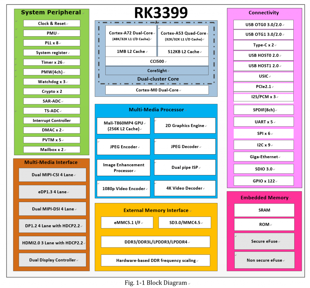
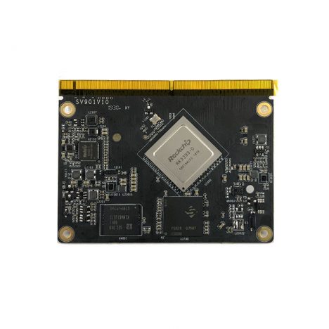
RK3399 is a low power, high performance processor for computing, personal mobile internet devices and other smart device applications. Based on Big.Little architecture, it integrates dual-core Cortex-A72 and quad-core Cortex-A53 with separate NEON coprocessor.
Many embedded powerful hardware engines provide optimized performance for high-end application. RK3399 supports multi-format video decoders including H.264/H.265/VP9up to4Kx2K@60fps, especially, H.264/H.265 decoders support 10bits coding, and also supports H.264/MVC/VP8 encoders by 1080p@30fps, high-quality JPEG encoder/decoder, and special image preprocessor and postprocessor.
Embedded 3D GPU makes RK3399 completely compatible with OpenGL ES1.1/2.0/3.0/3.1, OpenCL and DirectX 11.1. Special 2D hardware engine with MMU will maximize display performance and provide very smooth operation.
RK3399 has high-performance dual channel external memory interface (DDR3/DDR3L/LPDDR3/LPDDR4) capable of sustaining demanding memory bandwidths, also provides a complete set of peripheral interface to support very flexible applications.
1.2 Features
The features listed below which may or may not be present in actual product, may be subject to the third party licensing requirements. Please contact Rockchip for
actual product feature configurations and licensing requirements.
Microprocessor
- Dual-core ARM Cortex-A72 MPCore processor and Quad-core ARM Cortex-A53MPCore processor, both are high-performance, low-power and cached application processor
- Two CPU clusters.Big cluster with dual-coreCortex-A72 is optimized for high- performance and little cluster with quad-core Cortex-A53 is optimized for low
- Full implementation of the ARM architecture v8-A instruction set, ARM Neon Advanced SIMD (single instruction, multiple data) support for accelerating media and signal processing
- ARMv8 Cryptography Extensions
- SCU ensures memory coherency between the MPCore for each cluster
- CCI500 ensures the memory coherency between the two clusters
- Each Cortex-A72 integrates48KB L1 instruction cache and 32KB L1 data cache with 4- way set associative. Each Cortex A53 integrates 32KB L1 instruction cache and 32kB L1 data cache separately with 4-way set associative
- 1MB unified L2 Cache for Big cluster, 512KB unified L2 Cache for Little cluster
- Trustzone technology support
- Full Coresight debug solution
- Debug and trace visibility of whole systems
- ETM trace support
- Invasive and non-invasive debug
- Eight separate power domains for CPU core system to support internal power switch and externally turn on/off based on different application scenario
- PD_A72_B0: 1st Cortex-A72 + Neon + FPU + L1 I/D cache of big cluster
- PD_A72_B1: 2nd Cortex-A72+ Neon + FPU + L1 I/D cache of big cluster
- PD_SCU_B: SCU + L2 Cache controller, and including PD_A72_B0, PD_A72_B1, debug logic of big cluster
- PD_A53_L0: 1st Cortex-A53 + Neon + FPU + L1 I/D Cache of little cluster
- PD_A53_L1: 2nd Cortex-A53 + Neon + FPU + L1 I/D Cache of little cluster
- PD_A53_L2: 3rd Cortex-A53 + Neon + FPU + L1 I/D Cache of little cluster
- PD_A53_L3: 4th Cortex-A53 + Neon + FPU + L1 I/D Cache of little cluster
- PD_SCU_L: SCU + L2 Cache controller, and including PD_A53_L0, PD_A53_L1, PD_A53_L2, PD_A53_L3, debug logic of little cluster
- Two isolated voltage domain to support DVFS for big cluster and little cluster
1.2.2 Memory Organization
- Internal on-chip memory
- BootROM
- Internal SRAM
- External off-chip memory①
- DDR3/DDR3L/LPDDR3/LPDDR4
- SPI NOR/NAND Flash
- eMMC 1
- SD 3.0/MMC 51
1.2.3 Internal Memory
- Internal BootROM
- Size : 32KB
- Support system boot from the following device :
- SPI interface
- eMMC interface
- SD/MMC interface
- Support system code download by the following interface:
- USB OTG interface
- Internal SRAM
- Size : 200KB
- Support security and non-security access
- Security or non-security space is software programmable
- Security space can be 0KB,4KB,8KB,12KB,16KB,… up to 64KB by 4KB step
1.2.4 External Memory or Storage device
- Dynamic Memory Interface (DDR3/DDR3L/LPDDR3/LPDDR4)
- Compatible with JEDEC standard DDR3-1866 /DDR3L-1866 /LPDDR3-1866 / LPDDR4 SDRAM
- Support 2 channels, each channel is 16 or 32bits data width
- Support up to 2 ranks (chip selects) for each channel; totally 4GB(max) address space. Maximum address space of one rank in a channel is also 4GB, which is software-configurable
- 32bits/64bits data width is software programmable
- Programmable timing parameters to support DDR3/DDR3L/LPDDR3/LPDDR4 SDRAM from various vendor
- Advanced command reordering and scheduling to maximize bus utilization
- Embedded dynamic drift detection in the PHY to get dynamic drift compensation with the controller
- Programmable output and ODT impedance with dynamic PVT compensation
- Low power modes, such as power-down and self-refresh for DDR3/DDR3L/LPDDR3/LPDDR4 SDRAM
- Support standby mode to auto-gating DDR controller clock for power save
- Support power down DDR controller and DDR PHY
- Support hardware-based DDR frequency scaling
- eMMC Interface
- Fully compliant with JEDEC eMMC 5.1and eMMC 5.0 specification
- There is only one eMMC interface
- It is backward compliant with eMMC 4.51 and earlier versions
- Supports HS400, HS200, DDR50 and legacy operating
- Provide eMMC boot sequence to receive boot data from external eMMC device
- Configurable (Minimum 1 Block Size) FIFO used to aid data transfer between the CPU and the controller
- Handle the FIFO overrun and underrun condition by stopping interface clock
- Up to 3200Mbits per second data rate using 8 parallel data lines (eMMC HS400)
- Up to 1600Mbits per second data rate using 8 parallel data lines (eMMC HS200)
- Up to 832Mbits per second data rate using 8 parallel data lines (eMMC DDR52 mode)
- Transfers the data in 1 bit, 4 bit and 8 bit modes
- Cyclic Redundancy Check CRC7 for command and CRC16 for data integrity
- SD/MMC Interface
- Compatible with SD3.0, MMC 51
- There are 2 MMC interfaces which can be configured as SD/MMC or SDIO
- Support FIFO over-run and under-run prevention by stopping card clock automatically
- Support CRC generation and error detection
- Embedded clock frequency division control to provide programmable baud rate
- Support block size from 1 to 65535Bytes
- Data bus width is 4bits
1.2.5 System Component
- Cortex-M0
- Two Cortex-M0 inside RK3399 to cooperate with Cortex-A72/Cortex-A53
- Thumb instruction set combines high code density with 32-bit performance
- Integrated sleep modes for low power consumption
- Fast code execution permits slower processor clock or increases sleep mode time
- Deterministic, high-performance interrupt handling for time-critical applications
- Serial Wire Debug reduces the number of pins required for debugging
- CRU (clock & reset unit)
- Support clock gating control for individual components inside RK3399
- One oscillator with 24MHz clock input and 8 embedded PLLs
- Support global soft-reset control for whole SOC, also individual soft-reset for every components
- PMU (power management unit)
- Multiple configurable work modes to save power by different frequency or automatic clock gating control or power domain on/off control
- Lots of wakeup sources in different mode
- 6 separate voltage domains
- 30 separate power domains, which can be power up/down by software based on different application scenes
- Timer
- 14 on-chip 64bits Timers in SoC with interrupt-based operation for non-secure application
- 12 on-chip 64bits Timers in SoC with interrupt-based operation for secure application
- Provide two operation modes: free-running and user-defined count
- Support timer work state checkable
- Fixed 24MHz clock input
- PWM
- Four on-chip PWMs with interrupt-based operation
- Programmable pre-scaled operation to bus clock and then further scaled
- Embedded 32-bit timer/counter facility
- Support capture mode
- Support continuous mode or one-shot mode
- Provides reference mode and output various duty-cycle waveform
- Watchdog
- Three Watchdogs in SoC with 32 bits counter width
- Counter clock is from APB bus clock
- Counter counts down from a preset value to 0 to indicate the occurrence of a timeout
- WDT can perform two types of operations when timeout occurs:
- Generate a system reset
- First generate an interrupt and if this is not cleared by the service routine by the time a second timeout occurs then generate a system reset
- Programmable reset pulse length
- Totally 16 defined-ranges of main timeout period
- Mailbox
- Two Mailboxes in SoC to service multi-core communication
- Support four mailbox elements per mailbox, each element includes one data word, one command word register and one flag bit that can represent one interrupt
- Provide 32 lock registers for software to use to indicate whether mailbox is occupied
- Bus Architecture
- 128bit/64-bit/32-bit multi-layer AXI/AHB/APB composite bus architecture
- CCI500 embedded to support two clusters cache coherency
- 5 embedded AXI interconnect
- PERI low performance interconnect with one 128-bits AXI master, seven 64-bits AXI masters, one 32-bits AXI master, two 64-bits AXI slaves, five 32-bits AHB masters and lots of 32-bits AHB/APB slaves
- PERI high performance interconnect with one 128-bits AXI master, one 128-bits AXI slave, four 32-bits AHB masters and lots of 32-bits AHB/APB slaves
- DISPLAY interconnect with two 128-bits AXI masters, two 64-bits AXI masters, one 32-bits AXI master and lots of 32-bits AHB/APB slaves
- GPU interconnect with one 128-bits AXI master and 32-bits APB slave
- VIDEO interconnect with two 128-bits AXI masters, two 64-bits AXI masters and four 32-bits AHB slaves
- Flexible different QoS solution to improve the utility of bus bandwidth
- Interrupt Controller
- Support 8 PPI interrupt source and 148 SPI interrupt sources input from different components inside RK3399
- Support 16 software-triggered interrupts
- Input interrupt level is fixed, high-level sensitive for SPI and low-level sensitive for PPI
- Support Locality-specific Peripheral Interrupts (LPIs). These interrupts are generated by a peripheral writing to a memory-mapped register in the controller
- Two AXI stream interrupt interfaces separately for each cluster
- Support different interrupt priority for each interrupt source, and they are always software-programmable
- DMAC
- Micro-code programming based DMA
- The specific instruction set provides flexibility for programming DMA transfers
- Linked list DMA function is supported to complete scatter-gather transfer
- Support internal instruction cache
- Embedded DMA manager thread
- Support data transfer types with memory-to-memory, memory-to-peripheral, peripheral-to-memory
- Signals the occurrence of various DMA events using the interrupt output signals
- Mapping relationship between each channel and different interrupt outputs is software-programmable
- Two embedded DMA controller, BUS_DMAC is for bus system, PERI_DMAC is for peripheral system
- DMAC0 features:
- 6 channels totally
- 10 hardware request from peripherals
- 2 interrupt output
- Dual APB slave interface for register configuration, designated as secure and non-secure
- Support Trustzone technology and programmable secure state for each DMA channel
- DMAC1 features:
- 8 channels totally
- 20 hardware request from peripherals
- 2 interrupt output
- Dual APB slave interface for register configuration, designated as secure and non-secure
- Support Trustzone technology and programmable secure state for each DMA channel
- Security system
- Support Trustzone technology for the following components inside RK3399
- Cortex-A72, support security and non-security mode, switch by software
- Cortex-A53, support security and non-security mode, switch by software
- Except Cortex-A72 and Cortex-A53, the other masters in the SoC can also support security and non-security mode by software-programmable
- Some slave components in SoC can only be addressed by security master and the other slave components can be addressed by security master or non- security master by software-programmable
- Internal memory, part of space is addressed only in security mode, detailed size is software-programmable together with TZMA (Trustzone memory adapter)
- External DDR space can be divided into eight parts; each part can be software- programmable to be addressed in security mode or non-security mode
- Support Trustzone technology for the following components inside RK3399
- Embedded dual-channel encryption and decryption engine
- Support AES 128/192/256 bits key mode, ECB/CBC/CTR/XTS chain mode, Slave/FIFO mode
- Support DES/3DES (ECB and CBC chain mode), 3DES (EDE/EEE key mode), Slave/FIFO mode
- Support SHA1/SHA256/MD5(with hardware padding) HASH function, FIFO mode only
- Support 160-bit Pseudo Random Number Generator (PRNG)
- Support 256-bit True Random Number Generator (TRNG)
- Support PKA 512/1024/2048 bit Exp Modulator
- Support security boot
- Support security debug
1.2.6 Video CODEC
- Video Decoder
- MMU embedded
- Real-time video decoder of MPEG-1, MPEG-2, MPEG-4, H.263, H.264, H.265, VC-1, VP9, VP8, MVC
- 264/AVC, Base/Main/High/High10 profile @ level 5.1; up to 4Kx2K @ 30fps
- 265/HEVC, Main/Main10 profile @ level 5.1 High-tier; up to 4Kx2K @ 60fps
- VP9, profile 0, up to 4Kx2K @ 60fps
- MPEG-1, ISO/IEC 11172-2, up to 1080P @ 60fps
- MPEG-2, ISO/IEC 13818-2, SP@ML, MP@HL, up to 1080P @ 60fps
- MPEG-4, ISO/IEC 14496-2, SP@L0-3, ASP@L0-5, up to 1080P @ 60fps
- VC-1, SP@ML, MP@HL, AP@L0-3, up to 1080P @ 60fps
- MVC is supported based on H.264 or H.265, up to 1080P @ 60fps
- Supports frame timeout interrupt, frame finish interrupt and bit stream error interrupt
- Error detection and concealment support for all video formats
- Output data format YUV420 semi-planar, YUV400(monochrome), YUV422 is supported by 264
- For MPEG-4, GMC (global motion compensation) not supported
- For VC-1, up-scaling and range mapping are supported in image post-processor
- For MPEG-4 SP/H.263, using a modified H.264 in-loop filter to implement deblocking filter in post-processor unit
- Video Encoder
- Support video encoder for H.264 UP to HP@level4.1, MVC and VP8
- MMU Embedded
- Only support I and P slices, not B slices
- Support error resilience based on constrained intra prediction and slices
- Input data format:
- YCbCr 4:2:0 planar
- YCbCr 4:2:0 semi-planar
- YCbYCr 4:2:2
- CbYCrY 4:2:2 interleaved
- RGB444 and BGR444
- RGB555 and BGR555
- RGB565 and BGR565
- RGB888 and BRG888
- RGB101010 and BRG101010
- Image size is from 96×96 to 1920×1080(Full HD)
- Maximum frame rate is up to 1920×1080@30FPS②
1.2.7 JPEG CODEC
- JPEG decoder
- Input JPEG file: YCbCr 4:0:0, 4:2:0, 4:2:2, 4:4:0, 4:1:1 and 4:4:4 sampling formats
- Output raw image: YCbCr 4:0:0, 4:2:0, 4:2:2, 4:4:0, 4:1:1 and 4:4:4 semi-planar
- Decoder size is from 48×48 to 8176×8176(66.8Mpixels)
- Support JPEG ROI (region of image) decode
- Maximum data rate④ is up to 76million pixels per second
- Embedded memory management unit(MMU)
- JPEG encoder
- Input raw image:
- YCbCr 4:2:0 planar
- YCbCr 4:2:0 semi-planar
- YCbYCr 4:2:2
- CbYCrY 4:2:2 interleaved
- RGB444 and BGR444
- RGB555 and BGR555
- Input raw image:
- RGB565 and BGR565
- RGB888 and BRG888
- RGB101010 and BRG101010
- Output JPEG file: JFIF file format 1.02 or Non-progressive JPEG
- Encoder image size up to 8192×8192(64million pixels) from 96×32
- Maximum data rate④ up to 90million pixels per second
- Embedded memory management unit(MMU)
1.2.8 Image Enhancement
- Image pre-processor
- Only used together with HD video encoder inside RK3399, not support stand-alone mode
- Provides RGB to YCbCr 4:2:0 color space conversion, compatible with BT601, BT709 or user defined coefficients
- Provides YCbCr4:2:2 to YCbCr4:2:0 color space conversion
- Support cropping operation from 8192×8192 to any supported encoding size
- Support rotation with 90 or 270 degrees
- Video stabilization
- Work in combined mode with HD video encoder inside RK3399 and stand-alone mode
- Adaptive motion compensation filter
- Support scene detection from video sequence, encodes key frame when scene change noticed
- Image Post-Processor (embedded inside video decoder)
- Combined with HD video decoder and JPEG decoder, post-processor can read input data directly from decoder output to reduce bus bandwidth
- Also work as a stand-alone mode, its input data is from image data stored in external memory
- Input data format:
- Any format generated by video decoder in combined mode
- YCbCr 4:2:0 semi-planar
- YCbCr 4:2:0 planar
- YCbYCr 4:2:2
- YCrYCb 4:2:2
- CbYCrY 4:2:2
- CrYCbY 4:2:2
- Output data format:
- YCbCr 4:2:0 semi-planar
- YCbYCr 4:2:2
- YCrYCb 4:2:2
- CbYCrY 4:2:2
- CrYCbY 4:2:2
- Fully configurable ARGB channel lengths and locations inside 32bits, such as ARGB8888, RGB565, ARGB4444
- Input image size:
- Combined mode: from 48×48 to 8176×8176 (66.8Mpixels)
- Stand-alone mode: width from 48 to 8176, height from 48 to 8176, and maximum size limited to 7Mpixels
- Step size is 16 pixels
- Output image size: from 16×16 to 1920×1088 (horizontal step size 8, vertical step size 2)
- Support image up-scaling:
- Bicubic polynomial interpolation with a four-tap horizontal kernel and a two-tap vertical kernel
- Arbitrary non-integer scaling ratio separately for both dimensions
- Maximum output width is 3x input width
- Maximum output height is 3x input height
- Support image down-scaling:
- Arbitrary non-integer scaling ratio separately for both dimensions
- Unlimited down-scaling ratio
- Support YUV to RGB color conversion, compatible with 601-5, BT.709 and user definable conversion coefficient
- Support dithering (2×2 ordered spatial dithering) for 4/5/6bit RGB channel precision
- Support programmable alpha channel and alpha blending operation with the following overlay input formats:
- 8bit alpha +YUV444, big endian channel order with AYUV8888
- 8bit alpha +24bit RGB, big endian channel order with ARGB8888
- Support de-interlacing with conditional spatial de-interlace filtering, only compatible with YUV420 input format
- Support RGB image contrast/brightness/color saturation adjustment
- Support image cropping & digital zoom only for JPEG or stand-alone mode
- Support picture in picture
- Support image rotation (horizontal flip, vertical flip, rotation 90,180 or 270 degrees)
- Image Enhancement-Processor (IEP)
- Image format
- Input data: XRGB/RGB565/YUV420/YUV422
- Output data: ARGB/RGB565/YUV420/YUV422
- The format ARGB/XRGB/RGB565/YUV support swap
- Support YUV semi-planar/planar
- Support BT601_l/BT601_f/BT709_l/BT709_f color space conversion
- Support RGB dither up/down conversion
- Support YUV up/down sampling conversion
- Max resolution for static image up to 8192×8192
- Max resolution for dynamic image
- De-interlace: 1920×1080
- Sampling noise reduction: 1920×1080
- Compression noise reduction: 4096×2304
- Enhancement: 4096×2304
- Enhancement
- Gamma adjustment with programmable mapping table
- Hue/Saturation/Brightness/Contrast enhancement
- Color enhancement with programmable coefficient
- Detail enhancement with filter matrix up to 7×7
- Edge enhancement with filter matrix up to 7×7
- Programmable difference table for detail enhancement
- Programmable distance table for detail and edge enhancement
- Noise reduction
- Compression noise reduction with filter matrix up to 7×7
- Programmable difference table for compression noise reduction
- Programmable distance table for compression noise reduction
- Spatial sampling noise reduction
- Temporal sampling noise reduction
- Optional coefficient for sampling noise reduction
- De-interlace
- Input 4 fields, output 2 frames mode
- Input 4 fields, output 1 frames mode
- Input 2 fields, output 1 frames mode
- Programmable motion detection coefficient
- Programmable high frequency factor
- Programmable edge interpolation parameter
- Source width up to 1920
- Embedded memory management unit(MMU)
- Image format
1.2.9 Graphics Engine
- 3D Graphics Engine:
- ARM Mali-T860MP4 GPU, support OpenGL ES1.1/2.0/3.0, OpenCL1.2, DirectX11.1 etc.
- Embedded 4 shader cores with shared hierarchical tiler
- Provide MMU and L2 Cache with 256KB size
- Image quality using double-precision FP64, and anti-aliasing capabilities
- 10-bit and 16-bit YUV input and output formats
- 2D Graphics Engine:
- Source format:
- ARGB/RGB888/RGB565/RGB4444/RGB5551/YUV420/YUV422(SupportYUV422S P10bit/YUV420SP10bit)
- Destination formats:
- ARGB/RGB888/RGB565/RGB4444/RGB5551/YUV420/YUV422(Support YVYU422/420 output)
- Max resolution: 8192×8192 source, 4096×4096 destination
- Block transfer and Transparency mode
- Color fill with gradient fill, and pattern fill
- Alpha blending modes including global alpha, per pixel alpha (color/alpha channel separately) and fading
- Arbitrary non-integer scaling ratio, from 1/16 to 16
- 0, 90, 180, 270-degree rotation, x-mirror, y-mirror & rotation operation
- ROP2, ROP3, ROP4
- Support 4k/64k page size MMU
- Source format:
1.2.10 Video IN/OUT
- Camera Interface
- One or two MIPI-CSI input interface
- Image Signal Processer
- There are two ISP (Image Sensor Processor) built-in
- Maximum input resolution of one ISP is 14M pixels
- Main scaler with pixel-accurate up-scaling and down-scaling to any resolution between 4416×3312 and 32×16 pixel in processing mode
- Self scaler with pixel-accurate up-scaling and down-scaling to any resolution between 1920×1080 and 32×16 pixel in processing mode
- support of semi planar NV21 color storage format
- support of independent image cropping on main and self-path
- ITU-R BT 601/656 compliant video interface supporting YCbCr or RGB Bayer data
- 12-bit camera interface
- 12-bit resolution per color component internally
- YCbCr 4:2:2 processing
- quantization and Huffman tables
- Windowing and frame synchronization
- Macro block line, frame end, capture error, data loss interrupts and sync. (h_start, v_start) interrupts
- Luminance/chrominance and chrominance blue/red swapping for YUV input signals
- Continuous resize support
- Color processing (contrast, saturation, brightness, hue, offset, range)
- Display-ready RGB output in self-picture path (RGB888, RGB666 and RGB565)
- Rotation unit in self-picture path (90°, 180°, 270° and h/v flipping) for RGB output
- Read port provided to read back a picture from system memory
- Simultaneous picture read back, resizing and storing through self path while main
- path captures the camera picture
- Black level compensation
- Four channel Lens shade correction (Vignetting)
- Auto focus measurement
- White balancing and black level measurement
- Auto exposure support by brightness measurement in 5×5 sub windows
- Defect pixel cluster correction unit (DPCC) supports on the fly and table based pixel correction
- De-noising pre filter (DPF)
- Enhanced color interpolation (RGB Bayer demosaicing)
- Chromatic aberration correction
- Combined edge sensitive Sharpening / Blurring filter (Noise filter)
- Color correction matrix (cross talk matrix)
- Global Tone Mapping with wide dynamic range unit (WDR)
- Image Stabilization support and Video Stabilization Measurement
- Flexible Histogram calculation
- Digital image effects (Emboss, Sketch, Sepia, B/W (Grayscale), Color Selection, Negative image, sharpening)
- Solarize effect through gamma correction
- Display Interface
- Embedded two VOP, output from the following display
- One or Two MIPI-DSI port
- One eDP port
- One DP port
- One HDMI port
- Support AFBC function co-operation with GPU
- decompress FB generated by GPU FBC
- support 2560×1600 UI
- support ARGB888, RGB888, RGB565
- output for one layer among WIN0/1/2/3
- only support one IFDBC block which can be used for WIN0/1/2/3 by configuration
- Embedded two VOP, output from the following display
- Video Output Processor(VOP_BIG)
- Display interface
- HDMI interface
- Support 480p/480i/576p/576i/720p/1080p/1080i/4k
- Support RGB/YUV420(up to 10bit) format
- DP interface
- Support progressive/interlace
- Support RGB/YUV420/YUV422/YUV444(up to 10bit) format
- MIPI interface
- MIPI DCS command mode
- Dual-MIPI
- EDP interface
- Max resolution
- Max input resolution:4096×2304
- Max output resolution:4096×2160
- Scanning timing 8192×4096
- Support configurable polarity of DCLK/HSYNC/VSYNC/DEN
- HDMI interface
- Display process
- CABC
- BCSH,10bit
- Support display data swap
- Support YUV2RGB transition and RGB2YUV transition
- Support YUV2YUV
- GAMMA
- Support blank display and black display
- Display interface
- Support standby mode
- X-MIRROR, Y-MIRROR for win0/win1/win2/win3/hwc
- scale down for TV over scan
- Layer process
- Background layer
- programmable 30-bit color
- Afbcd
- format: ARGB8888/RGB888/RGB565
- Support block split
- win_sel(win0/win1/win2/win3)
- Win0/Win1 layer
- Support data format
- RGB888, ARGB888, RGB565,
- YCbCr420SP, YCbCr422SP, CbCr444SP, YUYV420, YUYV422, YVYU420, YVYU422
- RGB(8bit), YUV(8bit/10bit), YVYU/YUYV(8bit)
- YUV clip
- Y-8bit: 16~235; UV-8bit: 16~240
- Y-10bit: 64~940; UV-10bit: 64~960
- CSC
- RGB2YUV, YUV2RGB, RGB2RGB, YUV2YUV
- Support max input resolution 4096×8192
- Support max output resolution 4096×2160
- Support virtual display
- Support 1/8 to 8 scaling-down and scaling-up engine
- scale up using Bicubic and bilinear
- scale down using bilinear and average
- per-pix alpha + scale
- Support data swap
- RGB/BPP: rb_swap
- YUV: mid_swap, uv_swap
- transparency color key, prior to alpha blending and fading
- Support fading/alpha blending
- Support interlace output
- Support data format
- Win2/Win3 layer
- Support data format
- RGB888, ARGB888, RGB565
- 8BPP
- little endian and big endian for BPP
- BYPASS and LUT mode(32bit LUT,8bit AA+8bit-RGB) for BPP
- CSC
- RGB2YUV, RGB2RGB
- 4 display regions
- only one region at one scanning line
- Support data swap
- RGB/BPP: rb_swap
- Support transparency color key, prior to alpha blending and fading
- Support fading/alpha blending
- Support interlace output
- Support data format
- Hardware Cursor layer
- Support data format
- RGB888, ARGB888, RGB565
- 8BPP
- little endian and big endian for BPP
- BYPASS and LUT mode(32bit LUT,8bit AA+8bit-RGB)for BPP
- CSC
- RGB2YUV
- Support data format
- Background layer
- Support four hwc size: 32×32,64×64,96×96,128×128
- Support 2 color modes: normal and reversed color
- Support fading/alpha blending
- Support displaying out of panel, right or bottom
- Support interlace output
- Support p2i
- Overlay
- support RGB and YUV domain overlay
- Support 6 layers, background/win0/win1/win2/win3/hwc
- Win0/Win1/Win2/Win3 overlay position exchangeable
- Alpha blending
- Support multi alpha blending modes
- Support pre-multiplied alpha
- Support global alpha and per_pix alpha
- Support 256 level alpha
- Layer0/layer1/layer2/layer3/hwc support alpha
- Write back
- Support format
- RGB565(8bit), RGB888P(8bit)
- YUV420(8bit)
- Support scale
- horizontal scale down using bilinear, 25~1.0
- vertical throw odd/even line
- Embedded memory management unit(MMU)
- Support format
- Video Output Processor(VOP_LIT)
- Display interface
- HDMI interface
- Support 480p/480i/576p/576i/720p/1080p/1080i
- Support RGB format
- DP interface
- Support progressive/interlace
- Support RGB/YUV420/YUV422/YUV444format
- MIPI interface
- MIPI DCS command mode
- Dual-MIPI
- EDP interface
- Max resolution
- Max input resolution:4096×2304
- Max output resolution:2560×1600
- Scanning timing 8192×4096
- Support configurable polarity of DCLK/HSYNC/VSYNC/DEN
- HDMI interface
- Display process
- CABC
- BCSH,10bit
- Support display data swap
- Support YUV2RGB transition and RGB2YUV transition
- Support YUV2YUV
- GAMMA
- Support blank display and black display
- Support standby mode
- X-MIRROR, Y-MIRROR for win0/win2/hwc
- scale down for TV overscan
- Layer process
- Background layer
- programmable30 bit color
- Win0 layer
- Background layer
- Display interface
- Support data format
- RGB888, ARGB888, RGB565,
- YCbCr420SP, YCbCr422SP, CbCr444SP, YUYV420, YUYV422, YVYU420, YVYU422
- RGB(8bit), YUV(8bit), YVYU/YUYV(8bit)
- YUV clip
- Y-8bit: 16~235; UV-8bit: 16~240
- CSC
- RGB2YUV, YUV2RGB, RGB2RGB, YUV2YUV
- Support max input resolution 4096×8192
- Support max output resolution 2560×1600
- Support virtual display
- Support 1/8 to 8 scaling-down and scaling-up engine
- scale up using Bicubic and bilinear
- scale down using bilinear and average
- per-pix alpha + scale
- Support data swap
- RGB/BPP: rb_swap
- YUV: mid_swap, uv_swap
- transparency color key, prior to alpha blending and fading
- Support fading/alpha blending
- Support interlace output
- Win2 layer
- Support data format
- RGB888, ARGB888, RGB565
- 8BPP
- little endian and big endian for BPP
- BYPASS and LUT mode(32bit LUT,8bit AA+8bit-RGB) for BPP
- CSC
- RGB2YUV, RGB2RGB
- 4 display regions
- only one region at one scanning line
- Support data swap
- RGB/BPP: rb_swap
- Support transparency color key, prior to alpha blending and fading
- Support fading/alpha blending
- Support interlace output
- Support data format
- Hardware Cursor layer
- Support data format
- RGB888, ARGB888, RGB565
- 8BPP
- little endian and big endian for BPP
- BYPASS and LUT mode(32bit LUT,8bit AA+8bit-RGB)for BPP
- CSC
- RGB2YUV
- Support four hwc size: 32×32,64×64,96×96,128×128
- Support 2 color modes: normal and reversed color
- Support fading/alpha blending
- Support displaying out of panel, right or bottom
- Support interlace output
- Support data format
- Support p2i
- Overlay
- support RGB and YUV domain overlay
- Support 4 layers, background/win0/win2/hwc
- Win0/Win2 overlay position exchangeable
- Alpha blending
- Support multi alpha blending modes
- Support pre-multiplied alpha
- Support global alpha and per_pix alpha
- Support 256 level alpha
- Layer0/layer2/hwc support alpha
- Embedded memory management unit(MMU)
1.2.11 HDMI
- Single Physical Layer PHY with support for HDMI 1.4 and 2.0 operation
- For HDMI operation, support for the following:
- HPD input analog comparator
- 5–600MHz input reference clock
- Up to 10-bit Deep Color modes
- Up to 18Gbps aggregate bandwidth
- Up to 1080p at 120Hz and 4kx2k at 60Hz HDTV display resolutions and up to QXGA graphic display resolutions
- 3-D video formats
- Link controller flexible interface with 30-, 60- or 120-bit SDR data access
- Support HDCP 4/2.2
1.2.12 MIPI PHY
- Embedded 3 MIPI PHY, MIPI0 only for DSI, MIPI1 for DSI or CSI, MIPI2 only for CSI
- Lane operation ranging from 80 Mbps to 1.5 Gbps in forward direction
- Each port has 4 data lane, providing up to 6.0 Gbps data rate
- Support 1080p@60fps output with single channel
- Support 2560×1600@60fps output with MIPI0 and MIPI1 dual channel
1.2.13 eDP PHY
- Compliant with eDPTM Specification, version 3
- Support RGB 6/8/10bitvideo format
- Up to 4 physical lanes of 2.7/1.62 Gbps/lane
- Support VESA DMT and CVT timing standards
- Fully support EIA/CEA-861Dvideo timing and Info Frame structure
- Hot plug and unplug detection and link status monitor
- Supports Panel Self Refresh(PSR)
1.2.14 DisplayPort
- Compliant with DisplayPort Specification, version 2
- Compliant with HDCP2.2 (and back compatible with 3)
- There is only one DisplayPort controller built-in RK3399 which is shared by 2 Type-C interface
- 25-600Mhz pixel clock
- Supports 8/10 bpp RGB, YCbCr422, YCbCr420formats
- Supports up to 4kx2k at 60Hz resolution
- Variety of audio formats–PCM and compressed, over I2S or SPDIF interfaces
- 1Mbps AUX channel
1.2.15 TYPE-C Interface
- Embedded 2 Type-C PHY
- Compliant with USB Type-C Specification, revision 1
- Compliant with USB Power Delivery Specification, revision 0
- Attach/detach detection and signaling as DFP, UFP and DRP
- Plug orientation/cable twist detection
- Enable/disable VBUS as DFP and DRP (when operating as DFP)
- VBUS detection as UFP and DRP (when operating as UFP)
- USB Power Delivery communication across the CC wire
- Support USB3.0 Type-C and DisplayPort 1.2 Alt Mode on USB Type-C. Two PMA TX-only lanes and two PMA half-duplex TX/RX lanes (can be configured as TX-only or RX-only)
- Up to 5Gbps data rate for 0
- Up to 5.4Gbps(HBR2) data rate for DP1.2, can support 1/2/4 lane mode
- Support DisplayPort AUX channel
1.2.16 Audio Interface
- I2S/PCM
- Three I2S/PCM in SoC
- I2S0/I2S2 support up to 8 channels TX and 8 channels RX. I2S1 supports up to 2 channels TX and 2 channels RX
- I2S2 is connected to HDMI and DisplayPort I2S0 and I2S1 are exposed for peripherals.
- Audio resolution from 16bits to 32bits
- Sample rate up to 192KHz
- Provides master and slave work mode, software configurable
- Support 3 I2S formats (normal, left-justified, right-justified)
- Support 4 PCM formats (early, late1, late2, late3)
- I2S and PCM mode cannot be used at the same time
- SPDIF
- Support two 16-bit audio data store together in one 32-bit wide location
- Support biphase format stereo audio data output
- Support 16 to 31-bit audio data left or right justified in 32-bit wide sample data buffer
- Support 16, 20, 24 bits audio data transfer in linear PCM mode
- Support non-linear PCM transfer
1.2.17 Connectivity
- SDIO interface
- Compatible with SDIO 3.0 protocol
- 4bits data bus width
- There are 2 total MMC interfaces which may be configured as SD/MMC or SDIO
- GMAC 10/100/1000M Ethernet Controller
- There is one Giga Ethernet interface
- Supports 10/100/1000-Mbps data transfer rates with the RGMII interfaces
- Supports 10/100-Mbps data transfer rates with the RMII interfaces
- Supports both full-duplex and half-duplex operation
- Preamble and start-of-frame data (SFD) insertion in Transmit, and deletion in Receive paths
- Automatic CRC and pad generation controllable on a per-frame basis
- Options for Automatic Pad/CRC Stripping on receive frames
- Programmable InterFrameGap (40-96 bit times in steps of 8)
- Supports a variety of flexible address filtering modes
- Separate 32-bit status returned for transmission and reception packets
- Supports IEEE 802.1Q VLAN tag detection for reception frames
- Support detection of LAN wake-up frames and AMD Magic Packet frames
- Support checksum off-load for received IPv4 and TCP packets encapsulated by the Ethernet frame
- Support checking IPv4 header checksum and TCP, UDP, or ICMP checksum encapsulated in IPv4 or IPv6 datagrams
- Comprehensive status reporting for normal operation and transfers with errors
- Automatic generation of PAUSE frame control or backpressure signal to the GMAC core based on Receive FIFO-fill (threshold configurable) level
- Handles automatic retransmission of Collision frames for transmission
- Discards frames on late collision, excessive collisions, excessive deferral and underrun conditions
- SPI Controller
- 6 on-chip SPI controllers are inside
- Support serial-master and serial-slave mode, software-configurable
- DMA-based or interrupt-based operation
- Embedded two 32x16bits FIFO for TX and RX operation respectively
- UART Controller
- 5 on-chip UART controllers inside RK3399
- DMA-based or interrupt-based operation
- Embedded two 64Bytes FIFO for TX and RX operation respectively
- Support 5bit,6bit,7bit,8bit serial data transmit or receive
- Standard asynchronous communication bits such as start,stop and parity
- Support different input clock for UART operation to get up to 4Mbps or other special baud rate
- Support non-integer clock divides for baud clock generation
- Support auto flow control mode for UART0 and UART3
- I2C controller
- 9 on-chip I2C controllers
- Multi-master I2C operation
- Support 7bits and 10bits address mode
- Serial 8bits oriented and bidirectional data transfers can be made
- Software programmable clock frequency
- Data on the I2C-bus can be transferred at rates of up to 100 kbit/s in the Standard- mode, up to 400 kbit/s in the Fast-mode or up to 1 Mbit/s in Fast-mode
- GPIO
- 5 groups of GPIO (GPIO0~GPIO4), totally have 122 GPIOs
- All of GPIOs can be used to generate interrupt to CPU
- GPIO0 and GPIO1 can be used to wakeup system from low-power mode
- The pull direction (pull-up or pull-down) for all of GPIOs are software- programmable
- All of GPIOs are always in input direction in default after power-on-reset
- The drive strength for all of GPIOs is software-programmable
- USB 0
- Embedded 2 USB 0 interfaces
- Compatible Specification
- Universal Serial Bus 3.0 Specification, Revision 0
- Universal Serial Bus Specification, Revision 0
- eXtensible Host Controller Interface for Universal Serial Bus (xHCI), Revision 1.1
- Support Control/Bulk (including stream)/Interrupt/Isochronous Transfer
- Simultaneous IN and OUT transfer for USB3.0, up to 8Gbps bandwidth
- Descriptor Caching and Data Pre-fetching
- 0 Device Features
- Up to 7 IN endpoints, including control endpoint 0
- Up to 6 OUT endpoints, including control endpoint 0
- Up to 13 endpoint transfer resources, each one for each endpoint
- Flexible endpoint configuration for multiple applications/USB set-configuration modes
- Hardware handles ERDY and burst
- Stream-based bulk endpoints with controller automatically initiating data movement
- Isochronous endpoints with isochronous data in data buffers
- Flexible Descriptor with rich set of features to support buffer interrupt moderation, multiple transfers, isochronous, control, and scattered buffering support
- USB 3.0 xHCI Host Features
- Support up to 64 devices
- Support 1 interrupter
- Support 1 USB2.0 port and 1 Super-Speed port
- Concurrent USB3.0/USB2.0 traffic, up to 8.48Gbps bandwidth
- Support standard or open-source xHCI and class driver
- Support xHCI Debug Capability
- USB 3.0 Dual-Role Device (DRD) Features
- Static Device operation
- Static Host operation
- 0/USB2.0 OTG A device and B device basing on ID
- UFP/DFP and Data Role Swap Defined in USB TypeC Specification
- Not support USB3.0/USB2.0 OTG session request protocol(SRP), host negotiation protocol(HNP) and Role Swap Protocol(RSP)
- USB 2.0 Host
- Embedded 2 USB 2.0 Host interfaces
- Compatible with USB 2.0Host specification
- Supports high-speed(480Mbps), full-speed(12Mbps) and low-speed(1.5Mbps) mode
- Provides 16 host mode channels
- Support periodic out channel in host mode
- PCIe
- One PCIe port in RK3399
- Compatible with PCI Express Base Specification Revision 1
- Dual operation mode: Root Complex(RC)and End Point(EP)
- Maximum link width is 4, single bi-directional Link interface
- Support 2.5GT/s serial data transmission rate per lane per direction
- Support DMA within the module, 2 channels, 2 RAM partitions, 2K bytes depth
- Support Resizable BAR Capability
- Support Single Physical PCI Functions in Endpoint Mode
- Support Legacy Interrupt and MSI and MSI-X interrupt
- Support Outbound and Inbound Address Translation
- Support 8 Virtual Functions attached to Physical Function
- Support PCI Express Active State Power Management (ASPM) state L0s and L1
- Support L1 Power Management Substate
- Support PCI Function power states D0, D1 and D3, and the corresponding link power states L0, L1 and L2
1.2.18 Others
- Temperature Sensor(TS-ADC)
- Embedded 2 channel TS-ADC in RK3399
- TS-ADC clock must be less than 800KHZ
- 10-bits TS-ADC up to 50KS/s sampling rate
- -40~125C temperature range and 5℃ temperature resolution
- SAR-ADC (Successive Approximation Register)
- 6-channel single-ended 10-bit SAR analog-to-digital converter
- SAR-ADC clock must be less than 13MHZ
- Conversion speed range is up to 1MS/s sampling rate
- eFuse
- Two 1024bits(32×32) high-density electrical Fuse are integrated in RK3399
- Support standby mode and power down mode
- Embedded power-switch
- Embedded four redundancy bits
- Package Type
- FCBGA828(body: 21mmx21mm; ball size: 0.35mm; ball pitch: 65mm)
Rockchip RK3399 Datasheet
