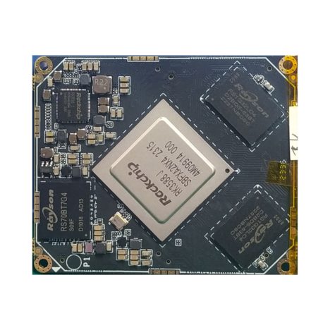
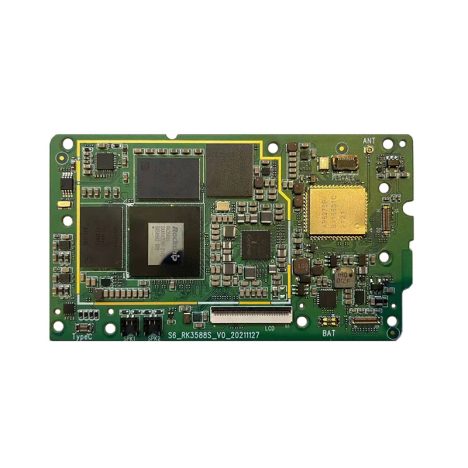
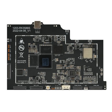
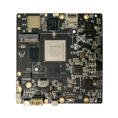
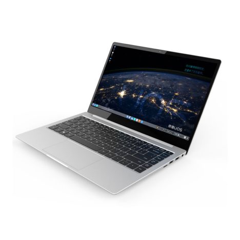
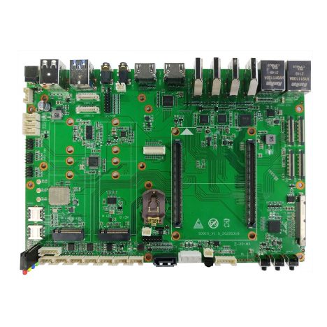
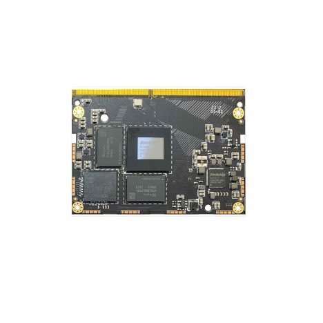
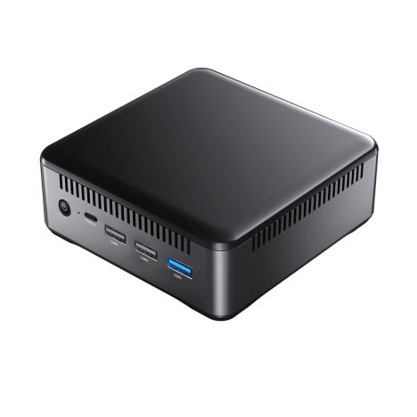
瑞芯微RK3588M是一款低功耗、高性能的处理器,采用8nm制程工艺,八核ARM架构设计,主要面向汽车电子、智能驾驶舱、车载娱乐系统、辅助驾驶等自动化应用。RK3588M已经通过车规质量认证,方便客户快速落地应用。本文将详细介绍RK3588M的规格参数(datasheet),帮助客户快速完成产品定义和功能设计。
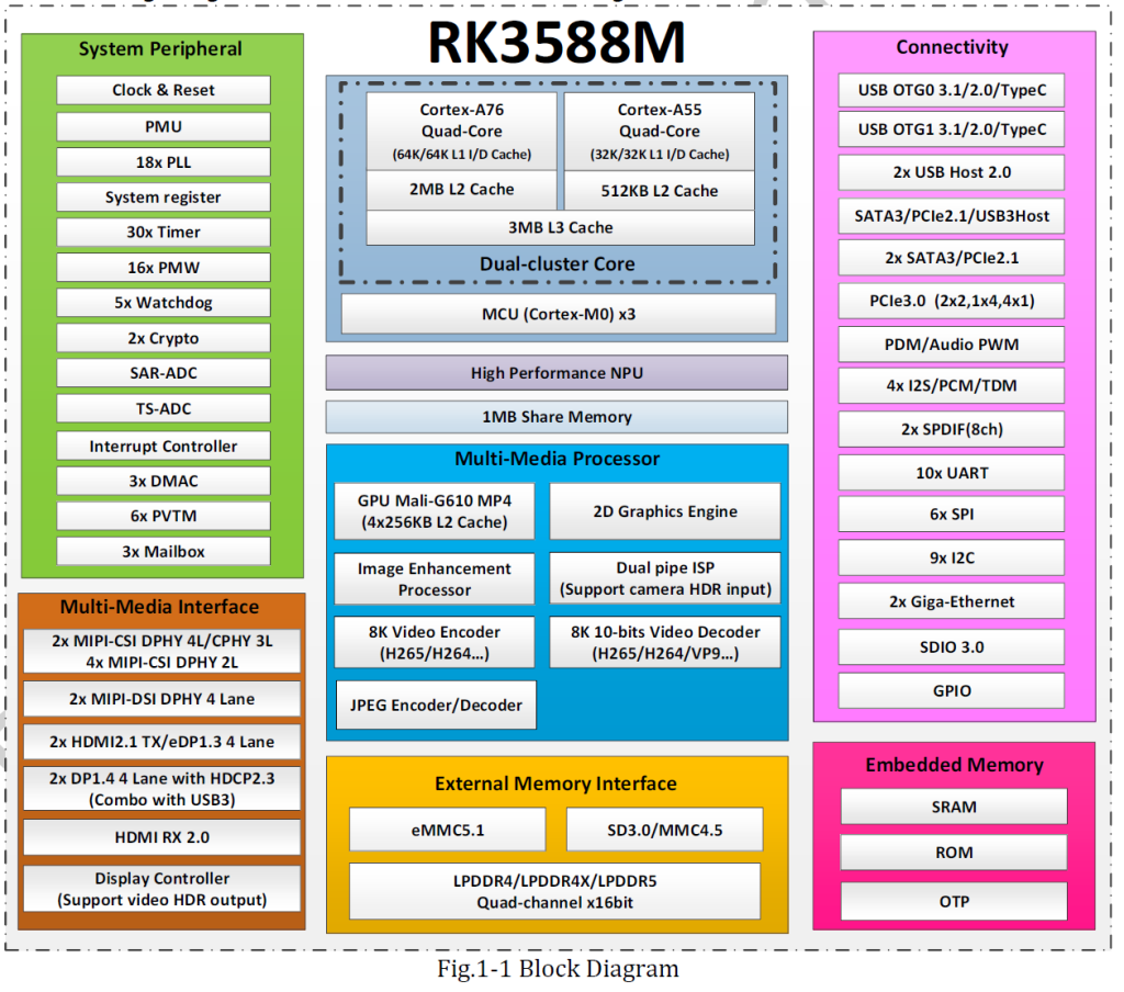 RK3588M将四核Cortex-A76和四核Cortex-A55与单独的NEON协处理器集成在一起。许多嵌入式强大的硬件引擎为高端应用程序提供了优化的性能。RK3588M通过以下方式支持H.265和VP9解码器8K@60fps,H.264解码器8K@30fps,和AV1解码器4K@60fps,还支持H.264和H.265编码器8K@30fps,高质量JPEG编码器/解码器,专门的图像预处理器和后处理器。嵌入式3D GPU使RK3588M与OpenGL ES 1.1、2.0和3.2、OpenCL高达2.2和Vulkan1.2完全兼容。带有MMU的特殊2D硬件引擎将最大限度地提高显示性能,并提供非常平稳的操作。
RK3588M引入了新一代完全基于硬件的最大4800万像素ISP(图像信号处理器)。它实现了许多算法加速器,如HDR、3A、LSC、3DNR、2DNR、锐化、去雾、鱼眼校正、伽玛校正等。内置NPU支持INT4/INT8/INT16/FP16混合操作,计算能力高达6TOPs。此外,由于其强大的兼容性,基于TensorFlow/MXNet/PyTorch/Caffe等一系列框架的网络模型可以轻松转换。
RK3588M具有高性能四通道外部存储器接口(LPDDR4/LPDDR4X/LPDDR5),能够维持苛刻的存储器带宽,还提供了一套完整的外围接口,以支持非常灵活的应用。
1.2.1 Microprocessor
Quad-core ARM Cortex-A76 MPCore processor and quad-core ARM Cortex-A55 MPCore processor, both are high-performance, low-power and cached application processor
DSU (DynamIQ Shared Unit) comprises the L3 memory system, control logic, and external interfaces to support a DynamIQ cluster
Full implementation of the ARM architecture v8-A instruction set, ARM Neon Advanced SIMD (single instruction, multiple data) support for accelerating media and signal processing
ARMv8 Cryptography Extensions
Trustzone technology support
Integrated 64KB L1 instruction cache, 64KB L1 data cache and 512KB L2 cache for each Cortex-A76
Integrated 32KB L1 instruction cache, 32KB L1 data cache and 128KB L2 cache for each Cortex-A55
Quad-core Cortex-A76 and Quad-core Cortex-A55 share 3MB L3 cache
Eight separate power domains for CPU core system to support internal power switch and externally turn on/off based on different application scenario
PD_CPU_0: 1st Cortex-A55 + Neon + FPU + L1/L2 I/D Cache
PD_CPU_1: 2nd Cortex-A55 + Neon + FPU + L1/L2 I/D Cache
PD_CPU_2: 3rd Cortex-A55 + Neon + FPU + L1/L2 I/D Cache
PD_CPU_3: 4th Cortex-A55 + Neon + FPU + L1/L2 I/D Cache
PD_CPU_4: 1st Cortex-A76 + Neon + FPU + L1/L2 I/D Cache
RK3588M Datasheet Rev 1.0 BY SCENSMART
PD_CPU_5: 2nd Cortex-A76 + Neon + FPU + L1/L2 I/D Cache
PD_CPU_6: 3rd Cortex-A76 + Neon + FPU + L1/L2 I/D Cache
PD_CPU_7: 4th Cortex-A76 + Neon + FPU + L1/L2 I/D Cache
Three isolated voltage domains to support DVFS, one for A76_0 and A76_1, one for A76_2 and A76_3, the other for DSU and Cortex-A55.
1.2.2 Memory Organization
Internal on-chip memory
BootRom
Support system boot from the following device:
SPI interface
eMMC interface
SD/MMC interface
Support system code download by the following interface:
USB OTG interface
Share Memory in the voltage domain of VD_LOGIC
PMU SRAM in VD_PMU for low power application
External off-chip memory
Dynamic Memory Interface
Compatible with JEDEC standards LPDDR4-4266/LPDDR4X-4266/LPDDR5-4800
Support four channels, each channel 16bits data widths
Support up to 2 ranks (chip selects) for each channel
Totally up to 32GB address space
Low power modes, such as power-down and self-refresh for SDRAM
eMMC Interface
Fully compliant with JEDEC eMMC 5.1 and eMMC 5.0 specification
Backward compliant with eMMC 4.51 and earlier versions specification.
Support HS400, HS200, DDR50 and legacy operating modes
Support three data bus width: 1bit, 4bits or 8bits
SD/MMC Interface
Compatible with SD3.0, MMC ver4.51
Data bus width is 4bits
Flexible Serial Flash Interface(FSPI)
Support transfer data from/to serial flash device
Support 1bit, 2bits or 4bits data bus width
Support 2 chips select
1.2.3 System Component
MCU
Three Cortex-M0 MCUs
MCU in VD_PMU integrate 16KB Cache and 16KB TCM
MCU in VD_NPU integrate 16KB Cache and 64KB TCM
MCU in PD_CENTER integrate 32KB TCM
Integrated Programmable Interrupt Controller, all IRQ lines connected to GIC for CPU also connect to MCU in VD_PMU(PMU_M0) and PD_CENTER(DDR_M0)
Integrated Debug Controller with JTAG interface
CRU (clock & reset unit)
Support total 18 PLLs to generate all clocks
One oscillator with 24MHz clock input
Support clock gating control for individual components
Support global soft-reset control for whole chip, also individual soft-reset for each component
PMU (power management unit)
Multiple configurable work modes to save power by different frequency or automatic clock gating control or power domain on/off control
Lots of wakeup sources in different mode
Support 10 separate voltage domains
Support 45 separate power domains, which can be power up/down by software based on different application scenes
RK3588M Datasheet Rev 1.0 BY SCENSMART
Timer
Support 12 secure timers with 64bits counter and interrupt-based operation
Support 18 non-secure timers with 64bits counter and interrupt-based operation
Support two operation modes: free-running and user-defined count for each timer
Support timer work state checkable
PWM
Support 16 on-chip PWMs(PWM0~PWM15) with interrupt-based operation
Programmable pre-scaled operation to bus clock and then further scaled
Embedded 32-bit timer/counter facility
Support capture mode
Support continuous mode or one-shot mode
Provides reference mode and output various duty-cycle waveform
Optimized for IR application for PWM3, PWM7, PWM11, PWM15
Watchdog
32-bit watchdog counter
Counter counts down from a preset value to 0 to indicate the occurrence of a timeout
WDT can perform two types of operations when timeout occurs:
Generate a system reset
First generate an interrupt and if this is not cleared by the service routine by the time a second timeout occurs then generate a system reset
Totally five Watchdog for CPU and MCU
Interrupt Controller
Support 12 PPI interrupt source and 480 SPI interrupt sources input from different components inside RK3588M
Support 16 software-triggered interrupts
Input interrupt level is fixed, high-level sensitive for SPI and low-level sensitive for PPI
Support different interrupt priority for each interrupt source, and they are always software-programmable
DMAC
Micro-code programming based DMA
Linked list DMA function is supported to complete scatter-gather transfer
Support data transfer types including memory-to-memory, memory-to-peripherals, peripherals-to-memory
Totally three embedded DMA controllers for peripheral system
Each DMAC features:
Support 8 channels
32 hardware request from peripherals
2 interrupt output
Support TrustZone technology and programmable secure state for each DMA channel
Secure System
Embedded two cipher engine
Support Link List Item (LLI) DMA transfer
Support SHA-1, SHA-256/224, SHA-512/384, MD5, SM3 with hardware padding
Support HMAC of SHA-1, SHA-256, SHA-512, MD5, SM3 with hardware padding
Support AES-128, AES-192, AES-256 encrypt & decrypt cipher
Support AES ECB/CBC/OFB/CFB/CTR/CTS/XTS/CCM/GCM/CBC-MAC/CMAC mode
Support SM4 ECB/CBC/OFB/CFB/CTR/CTS/XTS/CCM/GCM/CBC-MAC/CMAC mode
Support DES & TDES cipher, with ECB/CBC/OFB/CFB mode
Support up to 4096 bits PKA mathematical operations for RSA/ECC/SM2
Support generating random numbers
Support keyladder to guarantee key secure
Support data scrambling for all DDR types
RK3588M Datasheet Rev 1.0 BY SCENSMART
Support secure OTP
Support secure debug
Support secure DFT test
Support secure OS
Except CPU, the other masters in the SoC can also support security and non-security mode by software-programmable
Some slave components in SoC can only be addressed by security master and the other slave components can be addressed by security master or non-security master by software-programmable
System SRAM(share memory), part of space is addressed only in security mode
External DDR space can be divided into 16 parts, each part can be software-programmable to be enabled by each master
Mailbox
Three Mailbox in SoC to service CPU and MCU communication
Support four mailbox elements per mailbox, each element includes one data word, one command word register and one flag bit that can represent one interrupt
Provide 32 lock registers for software to use to indicate whether mailbox is occupied
Decompression
Support for decompressing GZIP files
Support for decompressing LZ4 files, including the General Structure of LZ4 Frame format and the Legacy Frame format.
Support for decompressing data in DEFLATE format
Support for decompressing data in ZLIB format
Support Hash32 check in LZ4 decompression process
Support the limit size function of the decompressed data to prevent the memory from being maliciously destroyed during the decompression process
1.2.4 Video CODEC
Video Decoder
Real-time video decoder of MPEG-1, MPEG-2, MPEG-4, H.263, H.264, H.265, VC-1, VP9, VP8, MVC, AV1
MMU Embedded
Multi-channel decoder in parallel for less resolution
H.264 AVC/MVC Main10 L6.0 : 8K@30fps (7680×4320)②②
VP9 Profile0/2 L6.1 : 8K@60fps (7680×4320)
H.265 HEVC/MVC Main10 L6.1 : 8K@60fps (7680×4320)
AVS2 Profile0/2 L10.2.6 : 8K@60fps (7680×4320)
AV1 Main Profile 8/10bit L5.3 : 4K@60fps (3840×2160)
MPEG-2 up to MP : 1080p@60fps (1920×1088)
MPEG-1 up to MP : 1080p@60fps (1920×1088)
VC-1 up to AP level 3 : 1080p@60fps (1920×1088)
VP8 version2 : 1080p@60fps (1920×1088)
Video Encoder
Real-time H.265/H.264 video encoding
Support up to 8K@30fps
Multi-channel encoder in parallel for less resolution
1.2.5 JPEG CODEC
JPEG Encoder
Baseline (DCT sequential)
Encoder size is from 96×96 to 8192×8192(67Mpixels)
Up to 90 million pixels per second
Embedded four encoder units
JPEG Decoder
Decoder size is from 48×48 to 65536×65536
Support YUV400/YUV411/YUV420/YUV422/YUV440/YUV444
Support up to 1080P@280fps, and 560 million pixels per second
Support MJPEG
RK3588M Datasheet Rev 1.0 BY SCENSMART
Embedded four encoder units
1.2.6 Neural Process Unit
Neural network acceleration engine with processing performance up to 6 TOPS
Include triple NPU core, and support triple core co-work, dual core co-work, and work independently Support integer 4, integer 8, integer 16, float 16, Bfloat 16 and tf32 operation Embedded 384KBx3 internal buffer Multi-task, multi-scenario in parallel
Support deep learning frameworks: TensorFlow, Caffe, Tflite, Pytorch, Onnx NN, Android NN, etc.
One isolated voltage domain to support DVFS
1.2.7 Graphics Engine
3D Graphics Engine
ARM Mali-G610 MP4
High performance OpenGLES 1.1, 2.0 and 3.2, OpenCL 2.2, Vulkan1.2 etc.
Embedded 4 shader cores with shared hierarchical tiler
Provide MMU and L2 Cache with 4x 256KB size
The latest Valhall architecture
ARM Frame Buffer Compression(AFBC) 1.3
Support Serial Wire debug for embedded MCU
One isolated voltage domain to support DVFS
2D Graphics Engine
Source format: ARGB/RGB888/RGB565/YUV420/YUV422/BPP
Destination formats: ARGB/RGB888/RGB565/YUV420/YUV422
Max resolution: 8192×8192 source, 4096×4096 destination
Block transfer and Transparency mode
Color fill with gradient fill, and pattern fill
Alpha blending modes including global alpha, per pixel alpha (color/alpha channel separately) and fading
Arbitrary non-integer scaling ratio, from 1/8 to 8
0, 90, 180, 270 degree rotation, x-mirror, y-mirror & rotation operation
ROP2, ROP3, ROP4
Support 4k/64k page size MMU
Image Enhancement Processor
Image format
Input data: YUV420/YUV422, semi-planar/planar, UV swap
Output data: YUV420/YUV422, semi-planar, UV swap, Tile mode
YUV down sampling conversion from 422 to 420
Max resolution for dynamic image up to 1920×1080
De-interlace
1.2.8 Video Input Interface
MIPI interface
Two MIPI DC(DPHY/CPHY) combo PHY
Support to use DPHY or CPHY
Each MIPI DPHY V1.2, 4lanes, 2.5Gbps per lane
Each MIPI CPHY V1.1, 3trios, 2.5Gsps per lane
Four MIPI CSI DPHY
Each MIPI DPHY V1.2, 2lanes, 2.5Gbps per lane
Support to combine 2 DPHY together to one 4lanes
Support camera input combination:
2 MIPI DCPHY + 4 MIPI CSI DPHY(2 lanes), totally support 6 cameras input
2 MIPI DCPHY + 1 MIPI CSI DPHY(4 lanes) + 2 MIPI CSI DPHY(2 lanes), totally support 5 cameras input
2 MIPI DCPHY + 2 MIPI CSI DPHY(4 lanes), totally support 4 cameras input
DVP interface
One 8/10/12/16-bit standard DVP interface, up to 150MHz input data
Support BT.601/BT.656 and BT.1120 VI interface
RK3588M Datasheet Rev 1.0 BY SCENSMART
Support the polarity of pixel_clk, hsync, vsync configurable
HDMI RX interface
Single-port HDMI 2.0 RX PHY, 4 lanes, no sideband channels
Data rate support in HDMI 2.0 mode
6Gbps down to 3.4Gbps
Data rate support in HDMI 1.4 mode
3.4Gbps down to 250Mbps
HDMI 2.0 video formats
TMDS Scrambler to enable support for 2160p@60 Hz with RGB/YCbCr4:4:4 or YCbCr4:2:2
Supports YCbCr 4:2:0 to enable 2160p@60Hz at lower HDMI link speeds
HDMI 1.4b video formats
All CEA-861-E video formats up to 1080p@120Hz
HDMI 1.4b 4K x 2K video formats(3840x2160p@24Hz/25Hz/30Hz and 4096x2160p@24Hz)
HDMI 1.4b 3D video modes with up to 340 MHz(TMDS clock)
Support HDCP2.3 and HDCP1.4
1.2.9 Image Signal Processor
Video Capture(VICAP)
Support BT601, BT656, BT1120
Support receiving six interfaces of MIPI CSI/DSI, up to four IDs for each interface
Support five CSI data formats: RAW8/10/12/14, YUV422
Support three modes of HDR: virtual channel mode, identification code mode, line counter mode
Support RAW data through to ISP0/1
Maximum input
48M::8064×6048@15 dual ISP
32M::6528×4898@30 dual ISP
16M::4672×3504@30 single ISP
3A: include AE/Histogram, AF, AWB statistics output
FPN: Fixed Pattern Noise removal
BLC: Black Level Correction
DPCC: Static/Dynamic defect pixel cluster correction
PDAF: Phase Detection Auto Focus
LSC: Lens shading correction
Bayer-2DNR: Spatial Bayer-raw De-noising
Bayer-3DNR: Temporal Bayer-raw De-noising
CAC: Chromatic Aberration Correction
HDR: 3-Frame Merge into High-Dynamic Range
DRC: HDR Dynamic Range Compression, Tone mapping
GIC: Green Imbalance Correction
Debayer: Advanced Adaptive Demosaic with Chromatic Aberration Correction
CCM/CSM: Color correction matrix; RGB2YUV etc
Gamma: Gamma out correction
Dehaze/Enhance: Automatic Dehaze and Effect enhancement
3DLUT: 3D-Lut Color Palette for Customer
LDCH: Lens-distortion only in the horizontal direction
YUV-2DNR: Spatial YUV De-noising
Sharp: Image Sharpening and boundary filtering
CMSK: privacy mask
GAIN: image local gain
Support multi-sensor reuse ISP
FishEye Correction(FEC)
Input mode and data format
Support RASTER: YUV422SP, YUV422I, YUV420SP
Output mode and data format
RASTER: YUV422SP, YUV422I, YUV420SP
RK3588M Datasheet Rev 1.0 BY SCENSMART
FBCE: YUV422SP, YUV420SP
Support 16×8, 32×16 two density
Support up to 4 times reduction factor
Resolution 128×128~4095×4095
Y Interpolation: Bicubic; C Interpolation: Biliner
1.2.10 Display interface
HDMI/eDP TX interface
Support two HDMI/eDP TX combo interface, but HDMI and eDP can not work at the same time for each interface
Support x1, x2 and x4 configuration for each interface
Support all the data rates for HDMI FRL: 3, 6, 8, 10 and 12Gbps
Support 1.62Gbps, 2.7Gbps and 5.4Gbps for eDP
Support up to 7680×4320@60Hz for HDMI TX, and 4K@60Hz for eDP
Support RGB/YUV(up to 10bit) format for HDMI TX
Support RGB, YCbCr 4:4:4, YCbCr 4:2:2 and 8/10 bit per component video format for eDP
Support DSC 1.2a for HDMI TX
Support HDCP2.3 for HDMI TX, and HDCP1.3 for eDP
DP TX interface
Support 2 DP TX 1.4a interface which combo with USB3.1 Gen1
Support 1/2/4lanes for each interface
Support 1.62Gbps, 2.7Gbps, 5.4Gbps and 8.1Gbps Serializer
Support up to 8192×4320@30Hz
Support RGB/YUV(up to 10bit) format
Support Single Stream Transport(SST)
Support DP Alt mode on USB Type-C
Support HDCP2.3, HDCP 1.3
MIPI DSI interface
Support 2 MIPI DPHY 2.0 interface
Support 4 data lanes and 4.5Gbps maximum data rate per lane
Support max resolution 4K@60Hz
Support dual MIPI display: left-right mode
Support RGB(up to 10bit) format
Support DSC 1.1/1.2a
BT.1120 video output interface
Support up to 1920×1080@60Hz
Support RGB(up to 8bit) format
Up to 150MHz data rate
1.2.11 Video Output Processor
Video ports
Video Port0, max output resolution: 7680×4320@60Hz
Video Port1, max output resolution: 4096×2304@60Hz
Video Port2, max output resolution: 4096×2304@60Hz
Video Port3, max output resolution: 1920×1080@60Hz
Cluster 0/1/2/3
Max input and output resolution 4096×2304
Support AFBCD
Support RGB/YUV/YUYV format
Support scale up/down ratio 4~1/4
Support rotation
ESMART 0/1/2/3
Max input and output resolution 4096×2304
Support RGB/YUV/YUYV format
Support scale up/down ratio 8~1/8
Support 4 region
Overlay
Support up to 8 layers overlay: 4 cluster/4 esmart
RK3588M Datasheet Rev 1.0 BY SCENSMART
Support RGB/YUV domain overlay
Post process
HDR
HDR10/HDR HLG
HDR2SDR/SDR2HDR
3D-LUT/P2I/CSC/BCSH/DITHER/CABC/GAMMA/COLORBAR
Write back
Format: ARGB8888/RGB888/RGB565/YUV420
Max resolution: 1920×1080
1.2.12 Audio Interface
I2S0/I2S1 with 8 channels
Up to 8 channels TX and 8 channels RX path
Audio resolution from 16bits to 32bits
Sample rate up to 192KHz
Provides master and slave work mode, software configurable
Support 3 I2S formats (normal, left-justified, right-justified)
Support 4 PCM formats (early, late1, late2, late3)
Support TDM normal, 1/2 cycle left shift, 1 cycle left shift, 2 cycle left shift, right shift mode serial audio data transfer
I2S, PCM and TDM mode cannot be used at the same time
I2S2/I2S3 with 2 channels
Up to 2 channels for TX and 2 channels RX path
Audio resolution from 16bits to 32bits
Sample rate up to 192KHz
Provides master and slave work mode, software configurable
Support 3 I2S formats (normal, left-justified, right-justified)
Support 4 PCM formats (early, late1, late2, late3)
I2S and PCM cannot be used at the same time
SPDIF0/SPDIF1
Support two 16-bit audio data store together in one 32-bit wide location
Support biphase format stereo audio data output
Support 16 to 31 bit audio data left or right justified in 32-bit wide sample data buffer
Support 16, 20, 24 bits audio data transfer in linear PCM mode
Support non-linear PCM transfer
PDM0/PDM1
Up to 8 channels
Audio resolution from 16bits to 24bits
Sample rate up to 192KHz
Support PDM master receive mode
Digital Audio Codec
Support 2 channels digital DAC
Support I2S/PCM interface, master and slave mode
Support 16 bit sample resolution
Support three modes of mixing for every digital DAC channel
Support volume control
VAD(Voice Activity Detection)
Support read voice data from I2S/PDM
Support voice amplitude detection
Support Multi-Mic array data storing
Support a level combined interrupt
1.2.13 Connectivity
SDIO interface
Compatible with SDIO3.0 protocol
4-bit data bus widths
GMAC 10/100/1000M Ethernet controller
Support two Ethernet controllers
RK3588M Datasheet Rev 1.0 BY SCENSMART
Support 10/100/1000-Mbps data transfer rates with the RGMII interfaces
Support 10/100-Mbps data transfer rates with the RMII interfaces
Support both full-duplex and half-duplex operation
USB3.1 Gen1
Support USB3.1 Gen1,equal to USB3.2 Gen1 and USB3.0,up to 5Gbps datarate
Embedded 2 USB3.1 OTG interfaces which combo with DP TX (USB3OTG_0 and USB3OTG_1)
Embedded 1 USB3.1 Host interface which combo with Combo PIPE PHY2 (USB3OTG_2)
Compatible Specification
Universal Serial Bus 3.0 Specification, Revision 1.0
Universal Serial Bus Specification, Revision 2.0 (exclude USB3OTG_2)
eXtensible Host Controller Interface for Universal Serial Bus (xHCI), Revision 1.1
Support Control/Bulk (including stream)/Interrupt/Isochronous Transfer
Simultaneous IN and OUT transfer for USB3.1 Gen1
Descriptor caching and data pre-fetching used to improve system performance in high-latency systems
LPM protocol in USB 2.0 (exclude USB3OTG_2) and U0, U1, U2, and U3 states for USB3.1 Gen1
USB3.1 Gen1 Device Features
Up to 10 IN endpoints, including control endpoint 0
Up to 6 OUT endpoints, including control endpoint 0
Up to 16 endpoint transfer resources, each one for each endpoint
Flexible endpoint configuration for multiple applications/USB set-configuration modes
Hardware handles ERDY and burst
Stream-based bulk endpoints with controller automatically initiating data movement
Isochronous endpoints with isochronous data in data buffers
Flexible Descriptor with rich set of features to support buffer interrupt moderation, multiple transfers, isochronous, control, and scattered buffering support
USB3.1 Gen1 xHCI Host Features
Support up to 64 devices
Support 1 interrupter
Support 1 USB2.0 port (exclude USB3OTG_2) and 1 Super-Speed port
Support standard or open-source xHCI and class driver
USB3.1 Gen1 Dual-Role Device (DRD) Features
Static Device Operation
Static Host Operation
USB3.1/USB2.0 OTG A device and B device basing on ID, USB3OTG_2 only support USB3.1 Gen1
Not Support USB3.1/USB2.0 OTG session request protocol (SRP), host negotiation protocol (HNP) and Role Swap Protocol (RSP)
Miscellaneous Features
USB2.0 PHY support Battery Charge detection
USB3OTG_0 and USB3OTG_1 support USB Type-C and DP Alt Mode
USB3OTG_2 PHY combos with PCIE and SATA
USB 2.0 Host
Compatible with USB 2.0 specification
Support two USB 2.0 Host
Supports high-speed(480Mbps), full-speed(12Mbps) and low-speed(1.5Mbps) mode
Support Enhanced Host Controller Interface Specification (EHCI), Revision 1.0
Support Open Host Controller Interface Specification (OHCI), Revision 1.0a
Combo PIPE PHY Interface
Support three Combo PIPE PHYs with PCIe2.1/SATA3.0/USB3.1 controller
RK3588M Datasheet Rev 1.0 BY SCENSMART
Combo PIPE PHY0 support one of the following interfaces
SATA
PCIe2.1
Combo PIPE PHY1 support one of the following interfaces
SATA
PCIe2.1
Combo PIPE PHY2 support one of the following interfaces
SATA
PCIe2.1
USB3.1 Gen1
PCIe2.1 Interface
Compatible with PCI Express Base Specification Revision 2.1
Support 1 lane for each PCIe2.1 interface
Support Root Complex(RC) only
Support 5Gbps data rate
SATA Interface
Compatible with Serial ATA 3.1 and AHCI revision 1.3.1
Support eSATA
Support 1 port for each SATA interface
Support 6Gbps data rate
PCIe3.0 Interface
Compatible with PCI Express Base Specification Revision 3.0
Support dual operation mode: Root Complex(RC) and End Point(EP)
Support data rates: 2.5Gbps(PCIe1.1), 5Gbps(PCIe2.1), 8Gps(PCIe3.0)
Support aggregation and bifurcation with 1x 4lanes, 2x 2lanes, 4x 1lanes and 1x 2lanes + 2x 1lanes
SPI interface
Support 5 SPI Controllers(SPI0-SPI4)
Support two chip-select output
Support serial-master and serial-slave mode, software-configurable
I2C Master controller
Support 9 I2C Master(I2C0-I2C8)
Support 7bits and 10bits address mode
Software programmable clock frequency
Data on the I2C-bus can be transferred at rates of up to 100k bits/s in the Standard-mode, up to 400k bits/s in the Fast-mode
UART interface
Support 10 UART interfaces(UART0-UART9)
Embedded two 64-byte FIFO for TX and RX operation respectively
Support 5bit, 6bit, 7bit, 8bit serial data transmit or receive
Standard asynchronous communication bits such as start, stop and parity
Support different input clock for UART operation to get up to 4Mbps baud rate
Support auto flow control mode for all UART
1.2.14 Others
Multiple group of GPIO
All of GPIOs can be used to generate interrupt
Support level trigger and edge trigger interrupt
Support configurable polarity of level trigger interrupt
Support configurable rising edge, falling edge and both edge trigger interrupt
Support configurable pull direction(a weak pull-up and a weak pull-down)
Support configurable drive strength
Temperature Sensor (TS-ADC)
Support User-Defined Mode and Automatic Mode
In User-Defined Mode, start_of_conversion can be controlled completely by software, and also can be generated by hardware.
In Automatic Mode, the temperature of alarm(high/low temperature) interrupt can be configurable
RK3588M Datasheet Rev 1.0 BY SCENSMART
In Automatic Mode, the temperature of system reset can be configurable
Support to 7 channel TS-ADC, the temperature criteria of each channel can be configurable
-40~125°C temperature range and 1°C temperature resolution
Successive approximation ADC (SARADC)
12-bit resolution
Up to 1MS/s sampling rate
8 single-ended input channels
OTP
Support 32Kbit space and higher 4k address space is non-secure part.
Support read and program word mask in secure model
Support maximum 32 bit OTP program operation
Support maximum 16 word OTP read operation
Program and Read state can be read
Program fail address record
Package Type
FCBGA1088L (body: 23mm x 23mm; ball size: 0.36mm; ball pitch: 0.65mm)
AEC-Q100 Grade 3
点击查看更多芯片的datasheet。
